

Semiconductor device
A semiconductor and conductive technology, applied in the direction of semiconductor devices, electrical components, circuits, etc., can solve problems such as application problems and easy generation of electromagnetic noise, and achieve the effect of suppressing changes and suppressing electromagnetic noise
- Summary
- Abstract
- Description
- Claims
- Application Information
AI Technical Summary
Problems solved by technology
Method used
Image

Examples
Embodiment approach 1
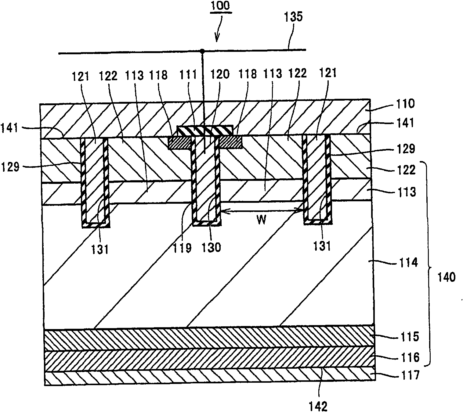
[0054] with the help of Figure 1 to Figure 4 , the semiconductor device according to the embodiment of the present invention will be described. figure 1 It is a cross-sectional view of the trench-type insulated gate semiconductor device 100 according to Embodiment 1 of the present invention. as it should figure 1 As shown, the trench type insulated gate semiconductor device 100 includes: a semiconductor substrate 140 having a main surface 141 and a main surface 142 opposite to the main surface 141; a conductivity type) n - semiconductor substrate (first impurity region) 114 ; p-type (second conductivity type) P collector layer (second impurity region) 116 formed on main surface 142 .
[0055] On the main surface 142 , a collector electrode 117 is formed, which is connected to the P collector layer 116 . Furthermore, in the semiconductor substrate 140, for the P collector layer 116, an n-type (first conductivity type) n layer is formed in a portion adjacent to the side opp...
Embodiment approach 2
[0088] with the help of Figure 5 to Figure 11 , the trench type insulated gate semiconductor device 100 and its manufacturing method according to the embodiment of the present invention will be described.
[0089] In addition, in Figure 5 to Figure 11 , for the above Figure 1 to Figure 4 The same or equivalent structures are assigned the same symbols and their descriptions are omitted.
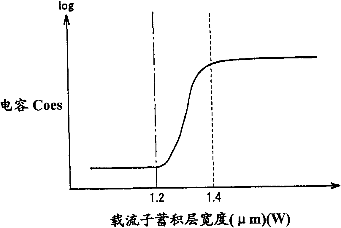
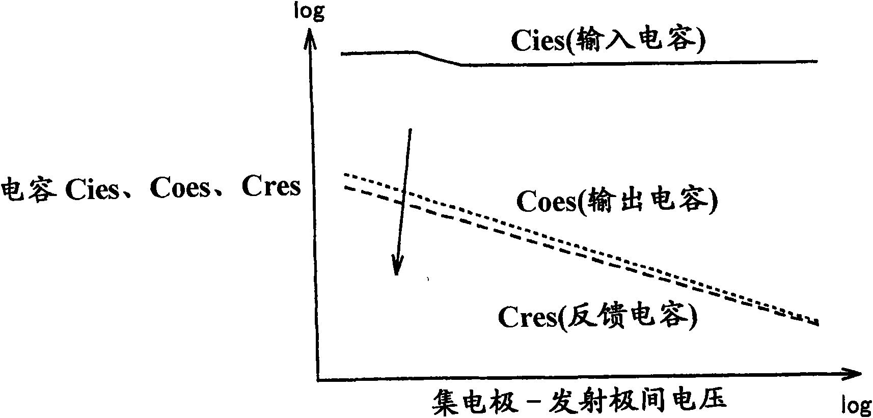
[0090] Figure 5 It is a cross-sectional view of trench-type insulated gate semiconductor device 100 according to Embodiment 2 of the present invention. as it should Figure 5 As shown, the unit (cell) 300 of the trench type insulated gate semiconductor device 100 has: the gate 120 connected to the gate wiring 135; the dummy gate 121 arranged at intervals on both sides of the gate 120; The P base region 122 connected to the emitter 110 between the gate 120 and the dummy gate 121 ; and the emitter layer 118 on the P base region 122 adjacent to the gate 120 on the left and right.
[009...
Embodiment approach 3
[0109] with the help of Figure 12 , the trench-type insulated gate semiconductor device 100 according to Embodiment 3 of the present invention will be described. In addition, in Figure 12 , for the above Figure 1 to Figure 11 The same or corresponding structures are assigned the same symbols, and descriptions thereof may be omitted.
[0110] as it should Figure 12 As shown, the trench type insulated gate semiconductor device 100 includes a plurality of cells 300 arranged at intervals.
[0111] The unit 300 has: a gate 120 connected to the gate wiring 135; a dummy gate 121 arranged at intervals on both sides of the gate 120; a P base region 122 located between the gate 120 and the dummy gate 121; and The emitter layer 118 on both sides of the gate 120 is formed on the P base region 122 . Then, a floating region (sixth impurity region) 112 is formed on the side opposite to the P base region 122 for the dummy gate 121 .
[0112] Here, a floating region 112 is formed bet...
PUM
 Abstract
Description
Claims
Application Information