Solid-state imaging device and imaging apparatus

a solid-state imaging and imaging apparatus technology, applied in the direction of radioation control devices, television system scanning details, television systems, etc., to achieve the effect of reducing external capacitance, storing charge quickly, and reducing power consumption of equipmen

Inactive Publication Date: 2014-01-14
SONY SEMICON SOLUTIONS CORP
View PDF18 Cites 22 Cited by
  • Summary
  • Abstract
  • Description
  • Claims
  • Application Information

AI Technical Summary

Benefits of technology

[0037]Thus, it is desirable to provide a solid-state imaging device and an imaging apparatus capable of speeding up activation operation and suppressing load change by performing suitable current supply in the occasion of activating the apparatus or in the occasion of sudden load change, thereby realizing speed-up of the operation and low power consumption.
[0040]The solid-state imaging device and the imaging apparatus according an embodiment of the invention detect level change of a prescribed supply voltage by the voltage supply means and performs control so that the level change is converged, therefore, there are advantages such as speed-up at the time of activation or that a sudden load change during operation can be minimum.
[0041]Therefore, for example, it is possible to allow the solid-state imaging device to be a stand-by state frequently because of the speed-up of activation, thereby realizing low power consumption of equipment. In addition, as a current supply due to the momentary load change, for example, an external capacitance is used. The current supply ability at the time of sudden load change is increased according to an embodiment of the invention, thereby storing charge to the external capacitance quickly, as a result, it is possible to select a smaller external capacitance and to expect improvement in aspects of costs and layout.
[0044]Additionally, the detection means is allowed to be the comparator which compares the supply voltage with the prescribed reference voltage, thereby realizing the device with the simple configuration. The detection means can be also an AD converter which digitalizes the supply voltage, thereby realizing the detection with high accuracy and in multistage.

Problems solved by technology

First, concerning a problem of the image sensor shown in FIG. 10, reset operation when charge storage is started to be the problem will be described as follows, focusing on the transfer transistor QT of the pixel 2. FIG. 14 is a timing chart of transfer-gate drive pulses applied to the transfer transistor QT from the vertical readout line.
First, when starting the reset operation, the reset transistor QR and the transfer transistor QT are turned on by signal pulses ΦR, ΦT from the reset line 11 and the vertical readout line 9 from the vertical scanning circuit 4 ((1) in the drawing). The photodiode PD and the detection region FD are reset because dark charge is swept out by the operation. Next, at the point of (2), the reset and transfer pulses ΦR, ΦT are set to the low level, the transfer transistor is turned off and the charge storage is started.

Method used


Image

  • Solid-state imaging device and imaging apparatus
  • Solid-state imaging device and imaging apparatus
  • Solid-state imaging device and imaging apparatus

Examples


first embodiment

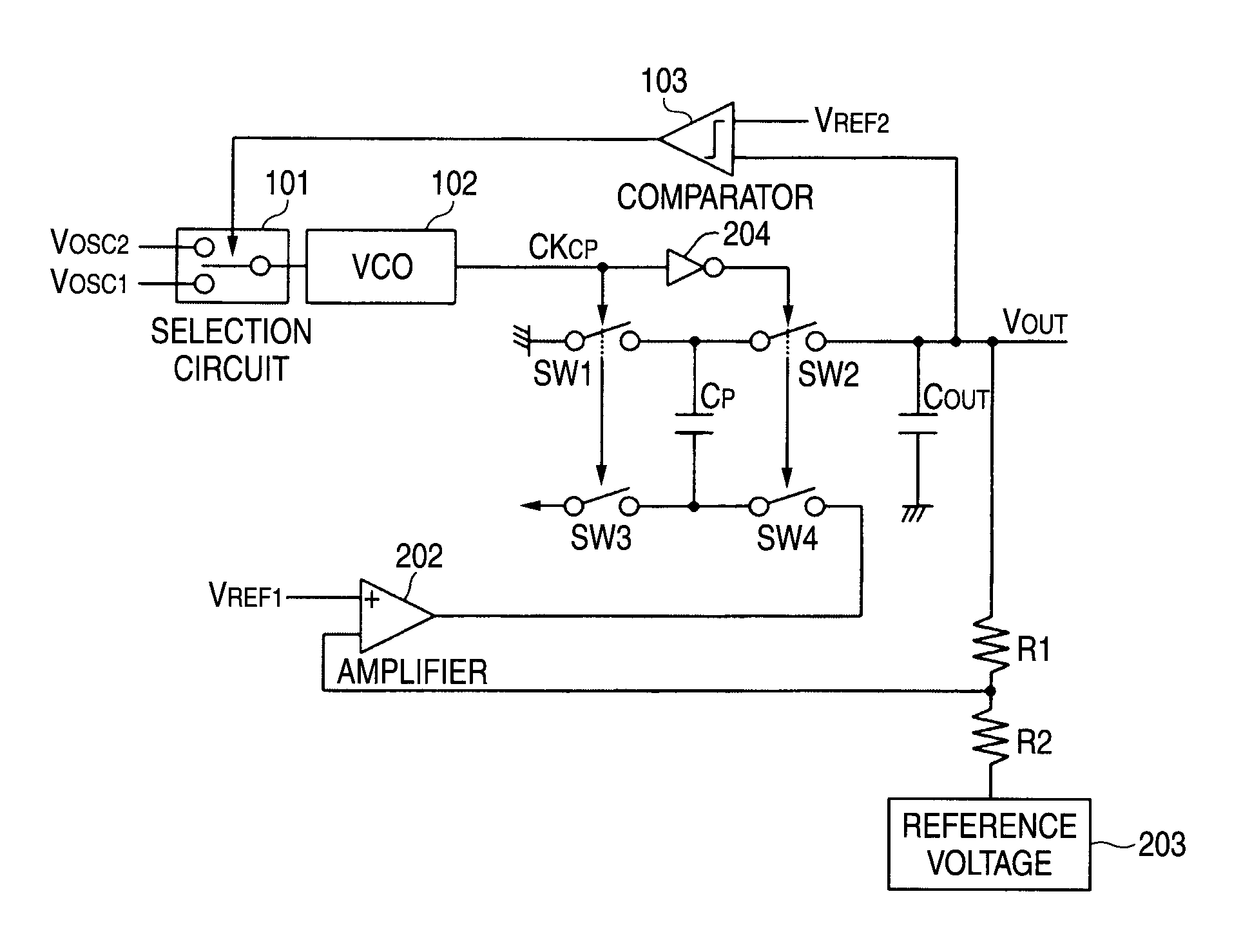
[0064]FIG. 1 is a circuit diagram showing a negative voltage generating circuit (charge pump circuit) of a solid-state imaging device according to an embodiment of the invention. The whole configuration of the solid-state imaging device is the same as the configuration, for example, shown in FIG. 10, and the explanation thereof is omitted. In FIG. 1, the same signs are put to components common to the related example shown in FIG. 13.

[0065]As shown in the drawing, the charge pump circuit includes a selection circuit 101, a voltage control oscillator (VCO) 102, a comparator 103, an amplifier 202, a reference voltage source 203, switches SW1 to SW4, voltage-dividing resistances R1, R2, a pump capacitor Cp, an output capacitor COUT, an inverter 204 and the like.

[0066]The operation as the charge pump is performed in the same manner as FIG. 13. First, charge is stored in the pump capacitor Cp by connecting between Vdd and GND by the switches SW1, SW3. After that, a negative voltage output...

second embodiment

[0075]FIG. 5 is a circuit diagram showing the charge pump circuit. The whole configuration of the solid-state imaging device is the same as the configuration shown, for example, in FIG. 10, and the explanation thereof is omitted. In FIG. 5, the same signs are put to components common to the embodiment shown in FIG. 1.

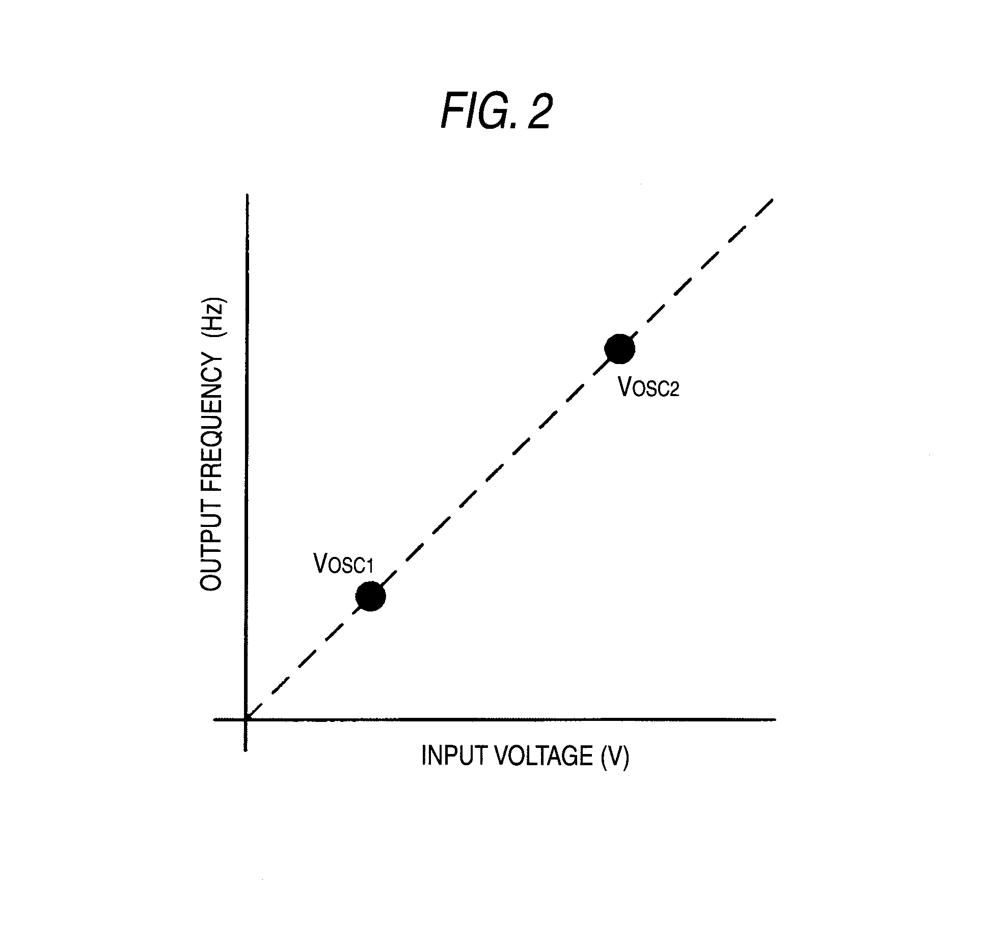
[0076]As shown in the drawing, in the charge pump circuit of the embodiment, the comparator 103 is replaced with the AD converter 113, as well as the selection circuit 101 is replaced with a selection circuit 111 which selects four voltage values VOSC1 to VOSC4. FIG. 6 is an explanatory graph showing input and output characteristics of the VCO 102 in the embodiment. As shown in the drawing, output signals having frequencies in relation to the level of the control voltages VOSC1, VOSC2, VOSC3, VOSC4 are outputted.

[0077]FIG. 7 and FIG. 8 are explanatory graphs showing operations of the embodiment. FIG. 7 shows the operation at the time of activation and FIG. 8 shows the o...

third embodiment

[0079]FIG. 9 is a circuit diagram showing the charge pump circuit. The whole configuration of the solid-state imaging device is the same as the configuration shown, for example, in FIG. 10, the explanation thereof is omitted. In FIG. 9, the same signs are put to components common to the embodiment shown in FIG. 5.

[0080]As shown in the drawing, in the charge pump circuit of the embodiment, the selection circuit 111 and the VCO 102 are replaced with a PLL 120, and an output frequency signal of the PLL 120 is variably controlled by a multiply control signal from the AD converter. Generally, it is necessary to correct frequency variations in the VCO due to process variations by using a particular correction method (for example, trimming and the like). The embodiment can be realized not using the particular correction since it is not necessary to use the VCO. As a result, frequency variations are reduced, thereby realizing a system in which band limitation for eliminating noise can be ea...


PUM


Abstract

A solid-state imaging device includes plural photoelectric conversion means arranged along light receiving surfaces, readout means for reading out signal charge generated in the photoelectric conversion means, a voltage supply means for supplying various levels of voltages to respective units including the photoelectric conversion means and the readout means, a detection means for detecting level change of a prescribed supply voltage in supply voltages by the voltage supply means and a control means for controlling so that the level change is converged when level change of the prescribed supply voltage is detected by the detection means.

Description

CROSS REFERENCE TO RELATED APPLICATIONS[0001]The present invention contains subject matter related to Japanese Patent Application JP 2006-321432 filed in the Japanese Patent Office on Nov. 29, 2006, the entire contents of which being incorporated herein by reference.BACKGROUND OF THE INVENTION[0002]1. Field of the Invention[0003]The invention relates to a solid-state imaging device used for various image sensors, particularly, relates to a solid-state imaging device and an imaging apparatus capable of securing efficient operation with respect to load changes at the time of activation and other occasions.[0004]2. Description of the Related Art[0005]In related arts, a MOS-type solid-state imaging device is known as this kind of solid-state imaging device. In the MOS-type solid-state imaging devices, a solid-state imaging device having a system in which signal charge of a photodiode (photoelectric converter) included in a pixel is read out after the charge is transferred to a detection...

Claims


Application Information

Patent Timeline
Patent Type & Authority Patents(United States)
IPC IPC(8): H04N5/378H04N5/374H04N5/335H04N5/217H04N5/376H04N5/369H04N5/225
CPCH04N5/23241H04N5/357H04N5/23245H04N5/335H04N5/369H02M3/07H02M3/071H04N23/651H04N23/667H04N25/00H04N25/60H04N25/70H01L27/146H04N25/76
Inventor KIKUCHI, MASARUWAKABAYASHI, HAYATO
Owner SONY SEMICON SOLUTIONS CORP
Why Eureka
Try Eureka