Photonic crystal thin plate type surface emitting annular beam laser

A photonic crystal and laser technology, applied in the structure of the optical resonator, the structure of the active area, etc., can solve the problem of low utilization rate of the light source, and achieve the effect of good polarization characteristics

Inactive Publication Date: 2009-11-25
INST OF SEMICONDUCTORS - CHINESE ACAD OF SCI
View PDF0 Cites 5 Cited by
  • Summary
  • Abstract
  • Description
  • Claims
  • Application Information

AI Technical Summary

Problems solved by technology

The surface-emitting laser obtained by the surface-emitting photonic crystal laser with edge is generally not single-polarized. To obtain polarized light, the easiest way is to add a polarizer, which has a low utilization rate of the light source.

Method used


Image

  • Photonic crystal thin plate type surface emitting annular beam laser
  • Photonic crystal thin plate type surface emitting annular beam laser
  • Photonic crystal thin plate type surface emitting annular beam laser

Examples


Embodiment Construction

[0027] In order to make the object, technical solution and advantages of the present invention clearer, the present invention will be described in further detail below in conjunction with specific embodiments and with reference to the accompanying drawings.

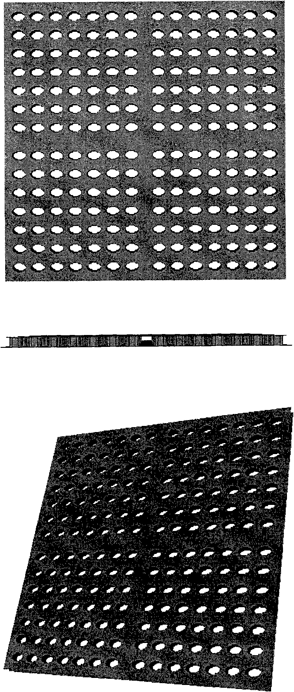
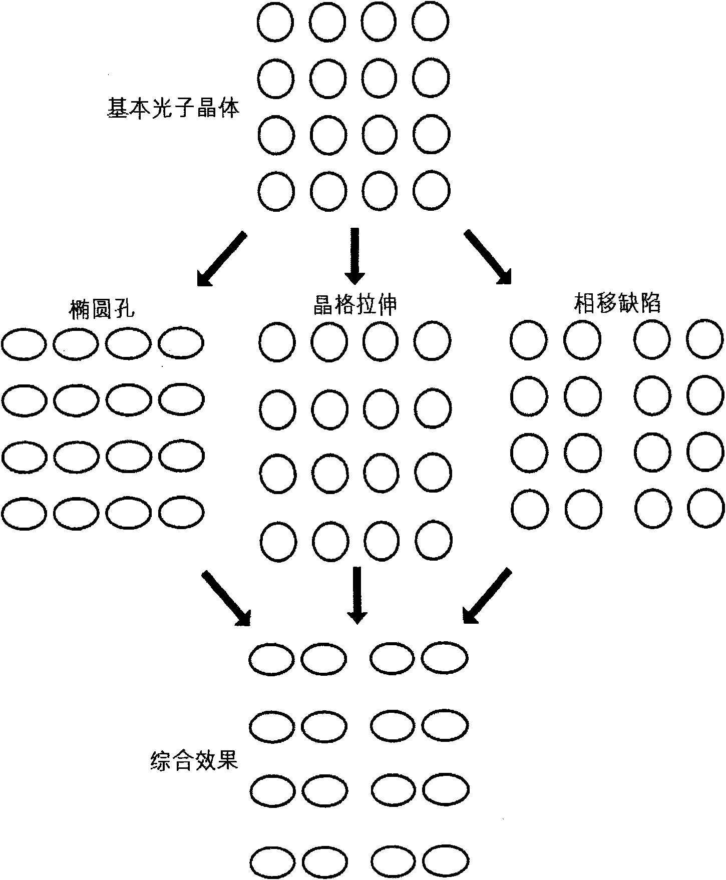
[0028] Such as figure 1 as shown, figure 1 The structural schematic diagram of the photonic crystal thin plate surface-emitting ring beam laser provided by the present invention includes a top view, a side view, and a view from a non-special perspective. The active region includes a photonic crystal structure and a phase shift defect; wherein, the photonic crystal structure unit in the active region is a circular hole or an elliptical hole, and the lattice structure is stretched to a certain extent, and a phase shift of an appropriate width is added defect.

[0029] In the material layer of the active area, etch out such as figure 2 Shown is a tetragonal lattice structure of circular holes or elliptical holes with pha...


PUM


Abstract

The invention discloses a photonic crystal thin plate type surface emitting annular beam laser. An active area of the laser comprises a photonic crystal structure and phase shift defects; and a photonic crystal structural unit in the active area is a round hole or an elliptical hole, and a lattice structure is stretched in certain degree, and is added with a phase shift defect with proper width. By utilizing the invention, the surface emitting laser with good polarization characteristics and prospected beams can be designed; and because of imperfect asymmetry when the photonic crystal structural unit is the elliptical hole, the optical-field distribution is changed, and further output light has good polarization characteristics.

Description

technical field [0001] The invention relates to the technical field of semiconductor optoelectronic devices, in particular to a photonic crystal thin plate surface emitting ring beam laser. Background technique [0002] Photonic crystals have been attracting people's attention since their concept was proposed. Its unique "photonic bandgap" (PBG) makes it a special place in laser applications, which can suppress the probability of spontaneous emission to produce photons with frequencies in the bandgap. When a certain defect is added to the photonic crystal, a defect state with a very narrow bandwidth may appear in the band gap, so that the probability of spontaneous emission to generate photons with a frequency in the defect state is not suppressed, and the spontaneous emission near this frequency also has a direction to the defect state. The probability of frequency conversion, which corresponds to the spontaneous emission of defect states, is enhanced. Through the design ...

Claims


Application Information

Patent Timeline
Patent Type & Authority Applications(China)
IPC IPC(8): H01S5/18H01S5/30
Inventor 郑婉华周文君陈微刘安金邢名欣
Owner INST OF SEMICONDUCTORS - CHINESE ACAD OF SCI
Why Eureka
Try Eureka