Circuit board and manufacture method thereof

A manufacturing method and circuit board technology, which is applied in the direction of multilayer circuit manufacturing, printed circuit components, and electrical connection formation of printed components, can solve problems such as multilayer circuit board 100 change, stress change, and influence, and improve yield , to avoid the effect of stress changes

Active Publication Date: 2009-12-09
UNIMICRON TECH CORP
View PDF0 Cites 5 Cited by
  • Summary
  • Abstract
  • Description
  • Claims
  • Application Information

AI Technical Summary

Problems solved by technology

[0008] However, the above-mentioned overall etching process used to reduce the thickness of the copper foil 114' is prone to stress changes, which in turn leads to changes in the dimension scale of the multilayer circuit board 100.
This will have a negative impact on the yield rate of the multilayer circuit board 100, thereby reducing the yield rate of the multilayer circuit board 100.

Method used


Image

  • Circuit board and manufacture method thereof
  • Circuit board and manufacture method thereof
  • Circuit board and manufacture method thereof

Examples


Embodiment Construction

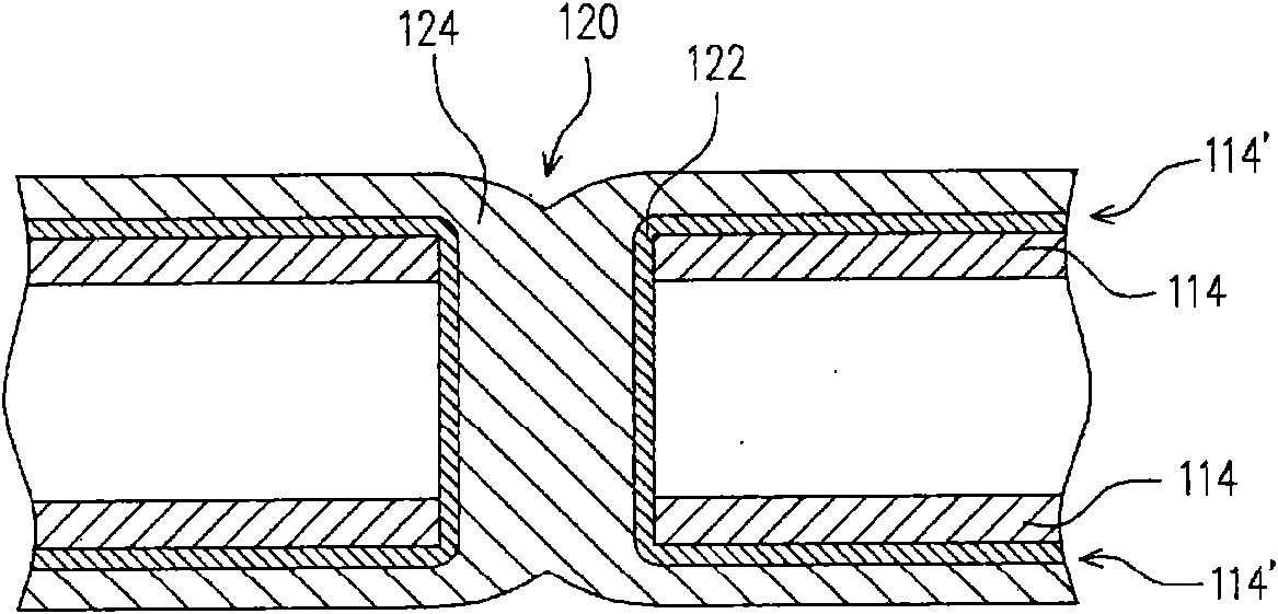
[0066] figure 2 It is a schematic cross-sectional view of a circuit board according to an embodiment of the present invention. see figure 2 , the circuit board 200 has at least one hole H1 , and the circuit board 200 includes a first circuit layer 210 , a second circuit layer 220 , an insulating layer 230 and a conductive connection structure 240 . The first circuit layer 210 and the second circuit layer 220 are disposed on opposite surfaces of the insulating layer 230 , that is, the insulating layer 230 is disposed between the first circuit layer 210 and the second circuit layer 220 . also, figure 2 The circuit board 200 shown can be regarded as a double sided circuit board or as one of the inner circuit substrates in a multilayer circuit board.

[0067] The hole H1 extends from the first circuit layer 210 to the second circuit layer 220, and the hole H1 may be a blind via or a through hole (such as figure 2 shown). The hole H1 has a hole wall S1, and the hole wall S...


PUM


Abstract

The invention relates to a manufacture method of a circuit board. The manufacture method comprises the following steps: firstly, providing a basal board comprising two conductive layers and an insulation layer arranged between the conductive layers; then, forming a hydrophobic film on one conductive layer; forming a hole extending form one conductive layer to the other conductive layer; forming a conductive connecting structure in the hole and connecting the conductive connecting structure between the conductive layers; removing the hydrophobic film after forming the conductive connecting structure; and finally, patterning the conductive layers to form two line layers.

Description

technical field [0001] The present invention relates to a circuit board and its manufacturing method, and in particular to a circuit board with at least two circuit layers and its manufacturing method. Background technique [0002] Today's multilayer circuit boards with at least two circuit layers usually have a conductive through hole structure, and the conductive through hole structure is electrically connected to two circuit layers of the multilayer circuit board, so that these circuit layers can Electrical conduction. At present, the methods of forming the conductive via structure mostly adopt mechanical drilling and via electroplating process, and after the conductive via structure is formed, the thickness of the second copper metal layer connecting the two ends of the conductive via structure will increase. Therefore, usually after the conductive via structure is formed, a full-surface etching process, which is the so-called thickness reduction process (also known as ...

Claims


Application Information

Patent Timeline
Patent Type & Authority Applications(China)
IPC IPC(8): H05K3/46H05K3/42H05K1/11
Inventor 张振铨
Owner UNIMICRON TECH CORP
Why Eureka
Try Eureka