Infrared detection method of faulty soldered joint of printing circuit board

A printed circuit board and infrared detection technology, which is applied in the field of infrared thermal imaging non-destructive detection of printed circuit board virtual solder joints, can solve the problem that the influence of solder joint appearance, volume and shape uncertainty cannot be ruled out, and it is not easy to load incident Accurate control of the angle, no obvious change in the surface temperature of the solder joints, etc., to achieve the effects of improved accuracy, easy operation, and strong versatility

Active Publication Date: 2009-12-30
BEIJING SATELLITE MFG FACTORY +1
View PDF1 Cites 22 Cited by
  • Summary
  • Abstract
  • Description
  • Claims
  • Application Information

AI Technical Summary

Problems solved by technology

At present, infrared thermal imaging non-destructive testing technology has been gradually applied to the detection of false solder joints on printed circuit boards. For example, the patent application number is 200710030000.6, and the title is "A device for on-line and defect identification of chip solder joints and chip packaging device". A method for on-line detection of chip solder joints. The method first passively heats the entire chip, then uses an infrared thermal imager to obtain a temperature map of the heated chip surface, and then processes the temperature map in three modes. Mode 1 passes the key The temperature value of the point is compared with the temperature criterion (preset temperature range) to determine whether there is a defect. Mode 2 locates the defect point according to the temperature difference between the temperature of the defect point and the normal point. Mode 3 locates the defect point according to the actual temperature value of the chip. To obtain performance parameters such as thermal resistance of the chip, the above detection method has the following disadvantages: Passive heating is used, and only the temperature change of the point where the solder joint is serious can be reflected, and most of the solder joints that are not serious are caused by the loading current. Insufficient heat, inconspicuous heat generation, or a small amount of heat generated inside is reflected to the outer surface of the solder joint through heat conduction radiation, resulting in insignificant temperature changes, resulting in insignificant changes in the surface temperature of the solder joint obtained by the infrared thermal imager. The appearance, volume, and shape of solder joints are different, so there are theoretical and technological deficiencies in the detection method based on actual temperature values
It can be seen that the detection by the method of temperature value difference analysis is contrary to the infinite difference in the appearance of solder joints. Now it is impossible to rule out the influence of solder joints on appearance, volume, and shape uncertainty, and it is difficult to accurately control the loading incident angle. The limitations of this detection method using absolute temperature values
[0005] Especially in the field of aerospace, due to the relatively harsh working conditions of spacecraft, higher requirements are put forward for the detection of virtual solder joints on circuit boards in various electronic devices carried on spacecraft. The existing absolute value points The detection method obviously cannot meet such high reliability requirements

Method used


Image

  • Infrared detection method of faulty soldered joint of printing circuit board
  • Infrared detection method of faulty soldered joint of printing circuit board
  • Infrared detection method of faulty soldered joint of printing circuit board

Examples


Embodiment Construction

[0024] The present invention will be further described below in conjunction with the accompanying drawings.

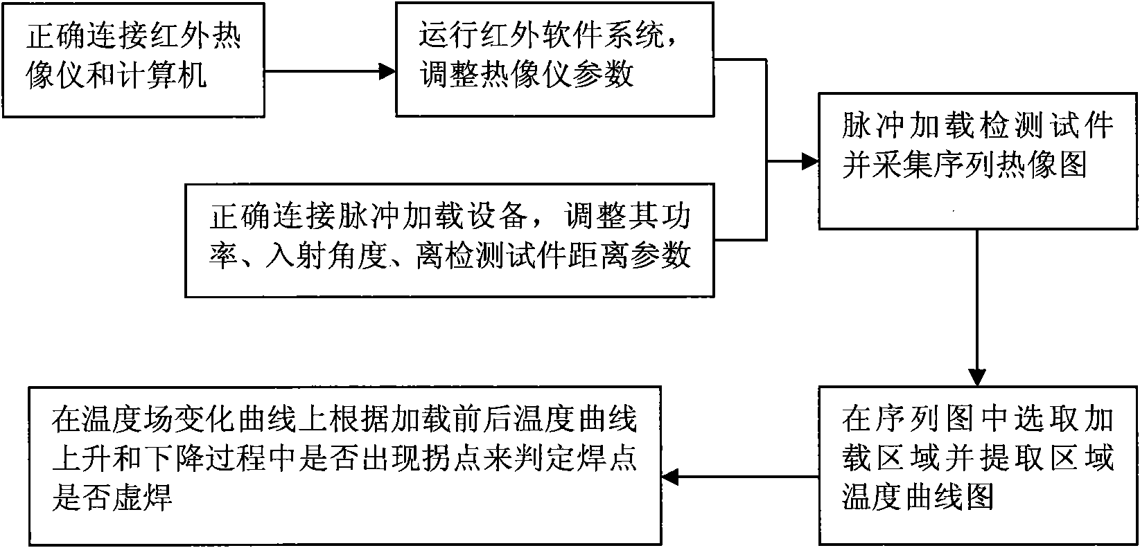
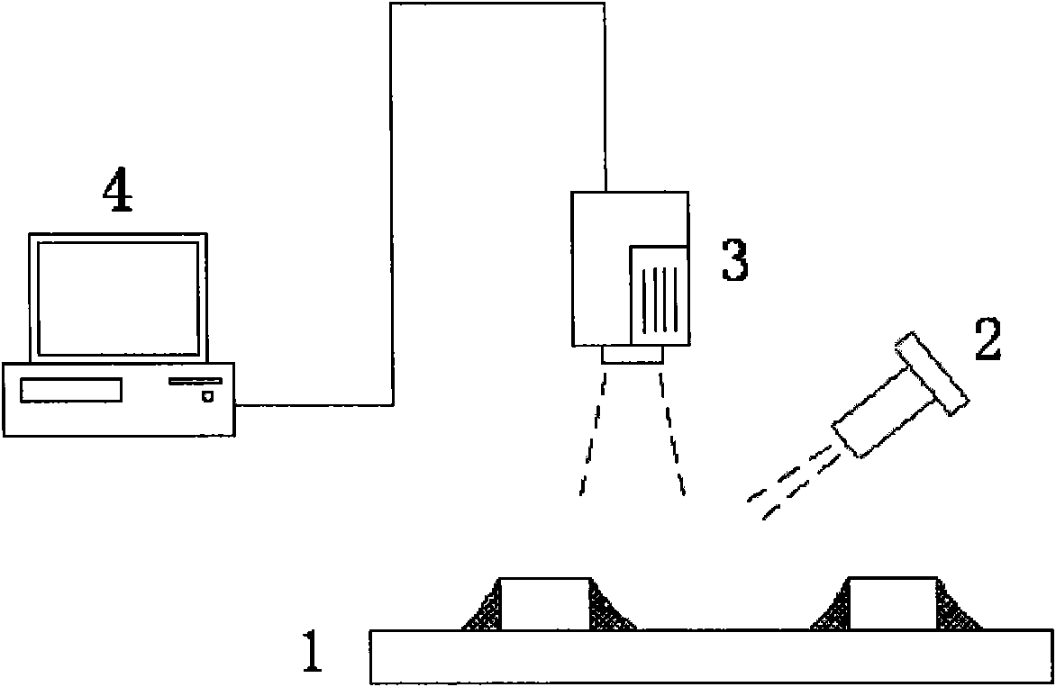
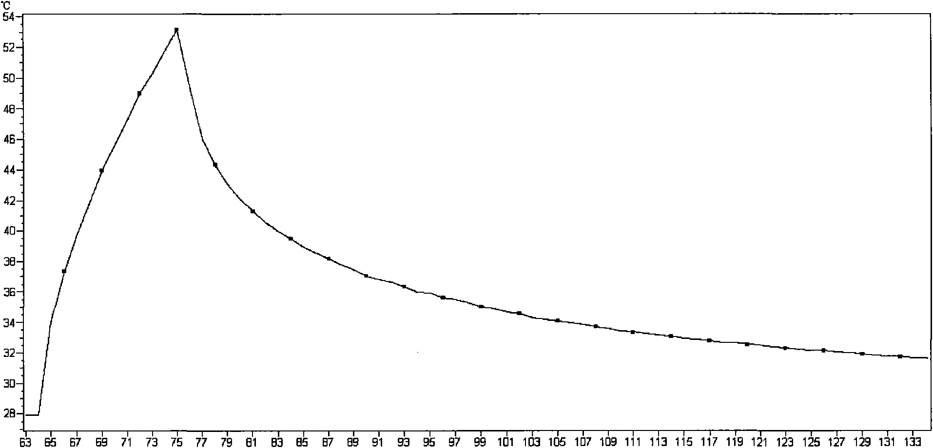
[0025] like figure 1 As shown, it is a scheme flow diagram of the detection method of the present invention, which mainly includes six steps. First, connect the thermal imaging camera and computer equipment correctly, see figure 2 ;Secondly, turn on the thermal imager and adjust its parameters, such as focal length, emissivity, sampling frequency, distance from the test piece, etc., wherein the acquisition frequency of the thermal imager is determined according to the rate of change of temperature; again, the pulse loading must be connected correctly equipment, adjust its power, incident angle, and distance parameters from the test piece, see figure 2 ; Next, pulse loading is performed on the test piece, and at the same time, the sequence thermal image is collected by the computer and stored on the hardware device; then, it is necessary to select the loaded area in...


PUM


Abstract

The invention relates to an infrared detection method of a faulty soldered joint of a printing circuit board. The infrared detection method comprises the following steps: firstly using an impulse heat loading device to carry out thermal loading to a detected solder joint, simultaneously using an infrared thermal image system to carry out continuous collection to the surface temperature of the detected solder joint in the thermal loading process and obtaining a sequence thermal image; then determining an area heated by the thermal loading device on the detected solder joint in the obtained sequence thermal image; then extracting a variation curve diagram of a temperature field of the area heated by the thermal loading device on the detected solder joint on the sequence thermal image before and after thermal loading; and finally judging whether the solder joint is a faulty soldered joint on the variation curve of the temperature field according to the process of rise and decrease of the temperature curve before and after loading. The infrared detection method can complete the detection to the faulty soldered joint by finding corner in the process of rise and decrease of the temperature curve, and has simple operation, high reliability and strong popularity.

Description

technical field [0001] The invention relates to an infrared thermal image non-destructive detection technology, in particular to an infrared thermal image non-destructive detection method for a printed circuit board virtual solder joint. Background technique [0002] Welding of solder joints is a common problem in the production process of printed circuit boards. The factors causing false joints of solder joints are very complicated. At present, it is impossible to eradicate them from the production process. The detection of solder joints is currently a worldwide problem. At present, the inspection methods of solder joints mainly include automatic optical inspection, automatic X-ray inspection, and flying probe test. The above three detection technologies have their own advantages and disadvantages and complement each other, but they are still unable to detect various types of solder joints, such as some cold solder joints, poor local wetting, and oily oxidation solder joint...

Claims


Application Information

Patent Timeline
Patent Type & Authority Applications(China)
IPC IPC(8): G01N25/72
Inventor 周双锋孔令超刘战捷王春青
Owner BEIJING SATELLITE MFG FACTORY
Why Eureka
Try Eureka