LED and production method thereof

A technology of light-emitting diodes and manufacturing methods, which is applied in semiconductor/solid-state device manufacturing, electrical components, electrical solid-state devices, etc., can solve problems such as contact displacement, displacement, poor bonding yield, etc. It is not easy to shift, and the joint is stable

Inactive Publication Date: 2010-01-06
ZHANJING TECH SHENZHEN +1
View PDF0 Cites 34 Cited by
  • Summary
  • Abstract
  • Description
  • Claims
  • Application Information

AI Technical Summary

Problems solved by technology

[0003] However, the bonding between the bonding layer 54 and the substrate 52 and the electrodes of the chip 53 is not strong enough, and the chip 53 is likely to be displaced relative to the substrate 52, resulting in poor electrical connection between the chip 53 and the substrate 52.
In addition, during the manufacturing process of the flip-chip LED 50 , the joint layer 54 will produce contact displacement between the substrate 52 and the chip 53 , resulting in poor joint yield.

Method used


Image

  • LED and production method thereof
  • LED and production method thereof
  • LED and production method thereof

Examples


Embodiment Construction

[0014] The present invention will be further described in detail below in conjunction with the accompanying drawings.

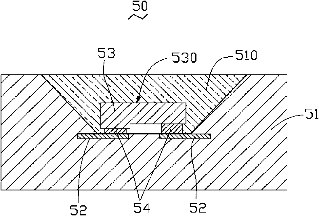
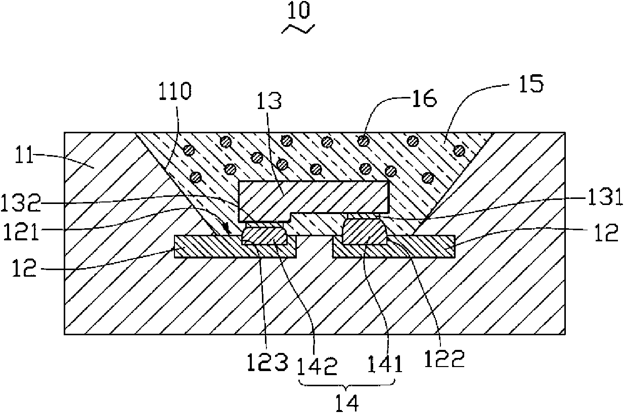
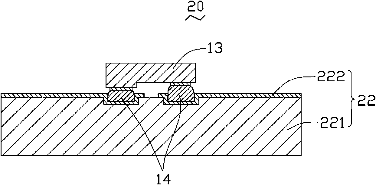
[0015] See figure 2 , the light emitting diode 10 provided by the first embodiment of the present invention includes a housing 11 , a substrate 12 , a light emitting diode chip 13 , a bonding layer 14 , and a packaging layer 15 .

[0016] The packaging case 11 has a receiving groove 110 . The material used for the packaging case 11 is an insulating material, such as liquid crystal polymer (Liquid Crystal Polymer), plastic, and the like.

[0017] The substrate 12 is disposed at the bottom of the containing groove 110 for carrying the LED chip 13 . The substrate 12 is connected to an external power source (not shown in the figure), so that the external power source conducts a driving current to the LED chip 13 through the substrate 12 . The substrate 12 is a lead frame, and its material is a high-conductivity material, such as gold, silver, copper and other...


PUM


Abstract

The invention relates to an LED and a production method thereof. The LED comprises a substrate, an LED wafer and a bonding layer, wherein the LED wafer is bonded on the substrate in a flip chip way; and the bonding layer is arranged between the substrate and the LED wafer so as to bond and electrically communicate the substrate and the LED wafer. The surface on which the substrate and the LED wafer are bonded is provided with at least one groove, the bonding layer is arranged on the groove. The bonding layer of the LED is arranged in the groove of the substrate, so that the LED wafer and the substrate are bonded firmly through the bonding layer, and the bonding layer is not prone to shift, thus ensuring that the LED wafer and the substrate have relatively good electric connection.

Description

technical field [0001] The invention relates to a light-emitting diode and a manufacturing method thereof, in particular to a flip-chip light-emitting diode and a manufacturing method thereof. Background technique [0002] Conventional methods of electrical bonding between a chip (chip) and a substrate (substrate) of a Light Emitting Diode (LED) generally include wire bonding and flip-chip bonding. see figure 1 , a chip-to-substrate flip-chip bonded light-emitting diode 50 , which includes a packaging case 51 , a substrate 52 and a chip 53 . The packaging case 51 has a receiving groove 510 , and the substrate 52 is disposed at the bottom of the receiving groove 510 . The surface of the wafer 53 having electrodes is bonded to the substrate 52 via the bonding layer 54 . The bonding layer 54 can be a bonding substance such as a metal bump (such as a gold bump) or a solder bump (Solder Bump). The electrodes of the chip 53 are bonded to the substrate 52 through the bonding la...

Claims


Application Information

Patent Timeline
Patent Type & Authority Applications(China)
IPC IPC(8): H01L33/00H01L23/488H01L21/60H01L33/44H01L33/62
CPCH01L2924/01023H01L33/44H01L2924/0105H01L2924/01082H01L24/81H01L2924/01047H01L2224/16237H01L2224/73204H01L2924/01049H01L2924/01079H01L24/17H01L2224/16H01L2924/01005H01L2924/01033H01L2924/01029H01L2924/10329H01L2224/83192H01L33/62H01L2224/14051H01L2924/01013H01L2224/81191H01L2224/0401H01L2224/06102H01L2224/1403H01L2224/1703H01L2924/12041H01L2924/00
Inventor 陈东安徐智鹏张忠民李泽安
Owner ZHANJING TECH SHENZHEN
Why Eureka
Try Eureka