Production method of encapsulated component of copper wire bonding IC chip

A chip packaging and bonding technology, used in electrical components, electrical solid devices, semiconductor devices, etc., can solve the problems of quality and reliability, restrict copper wire bonding packaging, IC chip pad craters, etc., and achieve savings The cost of gold wire bonding wire, good economic and social benefits, and the effect of strengthening the strength of solder joints

Inactive Publication Date: 2010-01-13
TIANSHUI HUATIAN TECH
View PDF0 Cites 20 Cited by
  • Summary
  • Abstract
  • Description
  • Claims
  • Application Information

AI Technical Summary

Problems solved by technology

[0003] The present invention aims to solve the problem of craters produced by copper wire bonding on IC chip pads, which has hidden dangers in quality and reliability, and restricts the technical problems of the promotion of copper wire bonding packaging to multi-pin and high-end products, thereby providing A simple and easy-to-use copper wire bonded IC chip package that can avoid craters

Method used


Image

  • Production method of encapsulated component of copper wire bonding IC chip
  • Production method of encapsulated component of copper wire bonding IC chip
  • Production method of encapsulated component of copper wire bonding IC chip

Examples


Embodiment 1

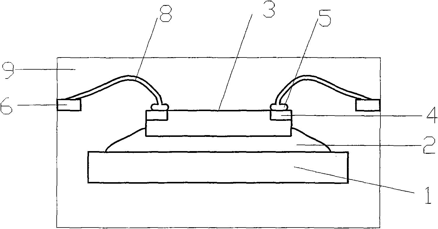
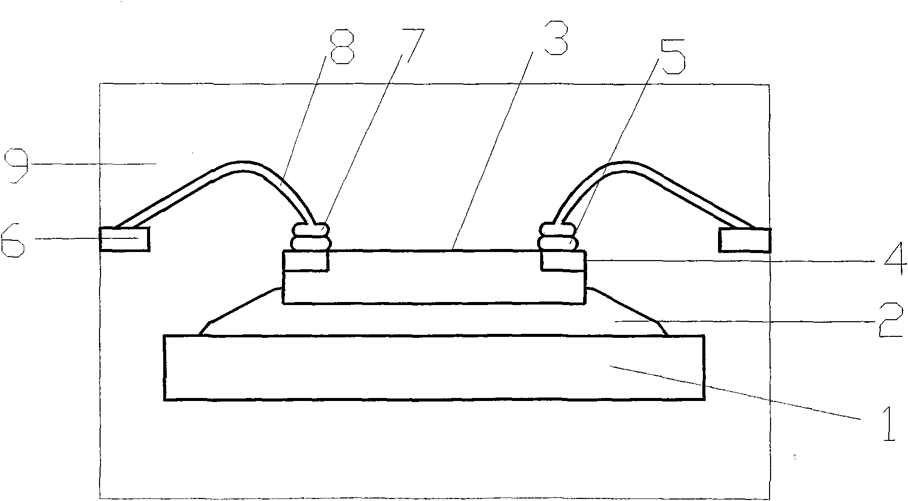
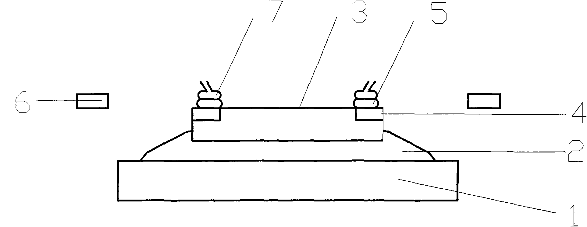
[0028] Thinning, scribing, core loading, plastic encapsulation, post-curing, rib cutting, electroplating, printing, forming separation, and packaging in the full-line process of the production method are the same as those of conventional gold wire and copper wire bonding packaging production, and the pressure welding operation The process is

[0029] 1. Plant golden ball

[0030] Fix the gold wire shaft on the pressure welding station, after the wire is threaded, the frame with the IC chip attached is automatically transferred to the track, and after preheating, it is transferred to the pressure welding fixture. Plant a golden ball on disc 4, and send the frame of the golden ball to the receiving folder after playing;

[0031] 2. Stack the ball

[0032] Fix the copper wire shaft on the pressure welding table, after threading the wire, automatically transfer the frame with gold balls to the track, and transfer it to the pressure welding fixture after preheating, and put gold ...


PUM


Abstract

The invention relates to a production method of an encapsulated component of a copper wire bonding IC chip. A welding plate of the IC chip is provided with a golden ball on which copper bonding balls are stacked, an arch wire is provided with a copper welding point on an inner pin of a lead frame, and a welding plate of the IC chip is connected with the pin of the lead frame. A plastic packaging body is covered on the IC chip, the copper balls stacked on the packed golden ball, the copper welding point of the arch wire on the inner pin of the lead frame and partial inner pins of the lead frame to form a whole circuit. The production method comprises wafer grinding, wafer scribing, core installing, press welding, plastic package, post curing, printing, punching separation, inspection, packaging and warehousing. The invention has simple and reasonable structure, easy use and high qualified rate in encapsulation and testing as well as high reliability, avoids craters, the intensity of the welding point is improved, the pull force of copper welding wires and the shearing strength of the welding point through the production method are greater than that in a copper (golden) bonding production method through direct wire threading, and unsoldering can not happen to the inner welding point.

Description

technical field [0001] The present invention relates to the technical field of electronic information automation components manufacturing, in particular to an IC chip integrated circuit package, specifically a copper wire bonded IC chip package, and the invention also includes a production method of the package. Background technique [0002] Although in the late 1980s and early 1990s, almost all semiconductor manufacturers were developing copper wire bonding, but due to yield problems and some limitations of copper wire itself, they failed to enter high-volume IC manufacturing. industry. At present, through the optimization of copper wire bonding process and important improvements in copper wire and supporting equipment, it has been mass-produced in IC chip packages with low-end and simple circuit designs. However, for multi-pin products, due to the complex circuit design under the IC chip pad (PAD), the craters generated during copper wire bonding will cause fatal damage t...

Claims


Application Information

Patent Timeline
Patent Type & Authority Applications(China)
IPC IPC(8): H01L23/495H01L23/482H01L23/488H01L21/60
CPCH01L2224/48091H01L2224/48465H01L2224/73265H01L2224/32245H01L2224/48482H01L24/48H01L2224/45147H01L2924/14H01L2924/181H01L2224/48499H01L2224/48247H01L2224/48H01L2224/45H01L2924/00014H01L2924/00H01L2924/00012H01L2924/01079
Inventor 常红军郭小伟慕蔚
Owner TIANSHUI HUATIAN TECH
Why Eureka
Try Eureka