Ion doping method for memory cell in DRAM

A technology of ion doping and memory cells, which is applied in the fields of electrical components, semiconductor/solid-state device manufacturing, circuits, etc., and can solve problems such as poor adhesion on the surface of silicon substrates

Active Publication Date: 2010-01-27
SEMICON MFG INT (SHANGHAI) CORP
View PDF0 Cites 0 Cited by
  • Summary
  • Abstract
  • Description
  • Claims
  • Application Information

AI Technical Summary

Problems solved by technology

[0005] The technical problem to be solved by the present invention is to provide an ion doping method for memory cells in DRAM to solve the problem of poor adhesion between photoresist and doped structure word line sidewalls and silicon substrate surface in the ion doping process of traditional memory cells

Method used


Image

  • Ion doping method for memory cell in DRAM
  • Ion doping method for memory cell in DRAM
  • Ion doping method for memory cell in DRAM

Examples


Embodiment Construction

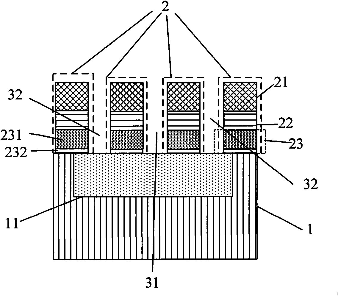
[0022] see figure 1 , the ion doping method of memory cell in DRAM of the present invention, wherein, memory cell has active region 11, and active region 11 is made in silicon substrate 1, and silicon substrate 1 is made with several word lines 2 of doping structure. Ion doping method of the present invention comprises the following steps:

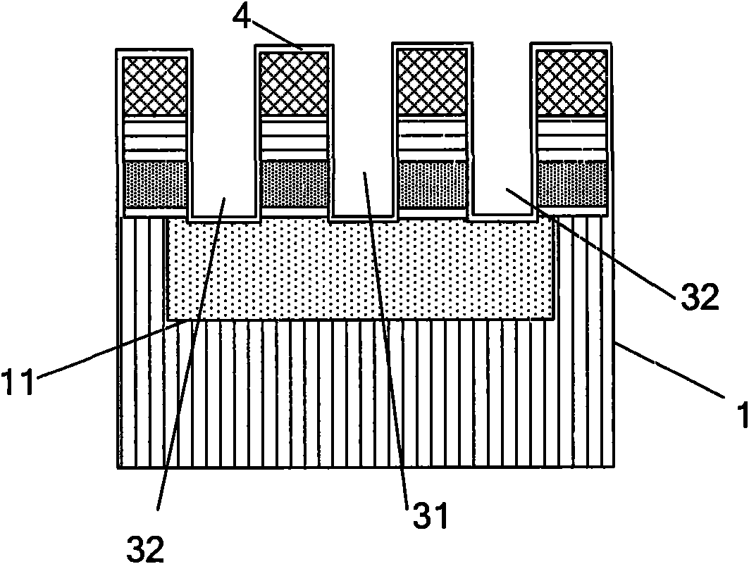
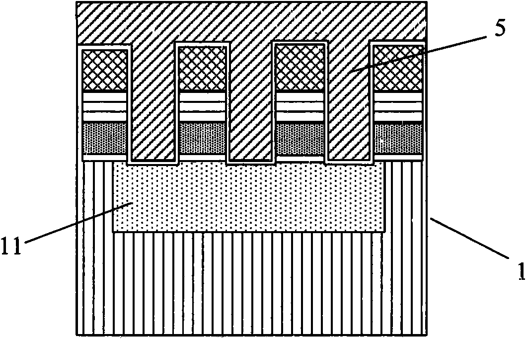
[0023] Step 1 see Figure 1~2 , oxidation figure 1 The surface and sidewall of the word line 2 with the doping structure shown, and the surface of the silicon substrate 1 between the word lines 2 with the doping structure. A thin layer of oxide 4 is formed on the entire surface of the memory cell device. see figure 1 The doped structure word line 2 includes a gate structure word line layer 23, a word line ohmic contact layer 22 and a word line mask layer 21 which are sequentially located on the surface of the active region of the silicon substrate 1; the gate structure word line layer 23 includes a layer which is sequentially located ...


PUM


Abstract

The invention relates to an ion doping method for a memory cell in a DRAM. The memory cell is provided with an active area produced in a silicon substrate and a plurality of doping structural word lines positioned on the surface of the active area in the silicon substrate. The method comprises the following steps: 1, oxidizing the surfaces and the side walls of the doping structural word lines and the surface of the silicon substrate among the doping structural word lines; 2, coating photoresists on the oxidized surfaces of the doping structural word lines and the oxidized surface of the silicon substrate; 3, removing the photoresists on the oxidized surface of the pre-doped silicon substrate among the doping structural word lines; and 4, filling pre-doping ions into the active area in the silicon substrate of which the photoresists are removed among the doping structural word lines. By oxidizing the surface of the memory cell directly before coating the photoresists, the ion doping method for the memory cell in the DRAM improves the adhesion of the memory cell with the photoresists and the uniformity of the photoresists, and solves the problems of poor adhesion of the photoresists and the surface of the memory cell and reduction of DRAM refreshing time caused by the poor adhesion in the conventional doping methods.

Description

technical field [0001] The invention relates to the field of manufacturing methods of dynamic random access memory (hereinafter referred to as DRAM), in particular to an ion doping method of memory cells in DRAM. Background technique [0002] With the development of the DRAM integrated manufacturing process, the critical dimension (Critical Dimension, CD) of each storage cell capacitor in the DRAM is also continuously reduced. The continuous shrinking of the size of the capacitor CD means that the capacitance value of the storage unit will continue to shrink. The development goal of DRAM market competition is to require the continuous increase of DRAM refresh time (Refresh Time) in order to reduce the refresh frequency of DRAM. However, the reduction of the capacitance value of DRAM storage unit runs counter to the development requirements of DRAM. Therefore, as the CD value of the storage unit capacitance in DRAM decreases, in order to meet the development requirements of ...

Claims


Application Information

Patent Timeline
Patent Type & Authority Applications(China)
IPC IPC(8): H01L21/8242H01L21/266
Inventor 彭坤
Owner SEMICON MFG INT (SHANGHAI) CORP
Why Eureka
Try Eureka