Organic electroluminescence device, process of producing organic electroluminescence device, and electronic apparatus
An electroluminescence device and electroluminescence technology, which are applied to electroluminescence light sources, electric light sources, lighting devices, etc., can solve the problems of cracking, low reliability of organic EL devices, and inability to follow the inorganic compound layer, and achieve high reliability. Effect
- Summary
- Abstract
- Description
- Claims
- Application Information
AI Technical Summary
Problems solved by technology
Method used
Image
Examples
no. 1 approach
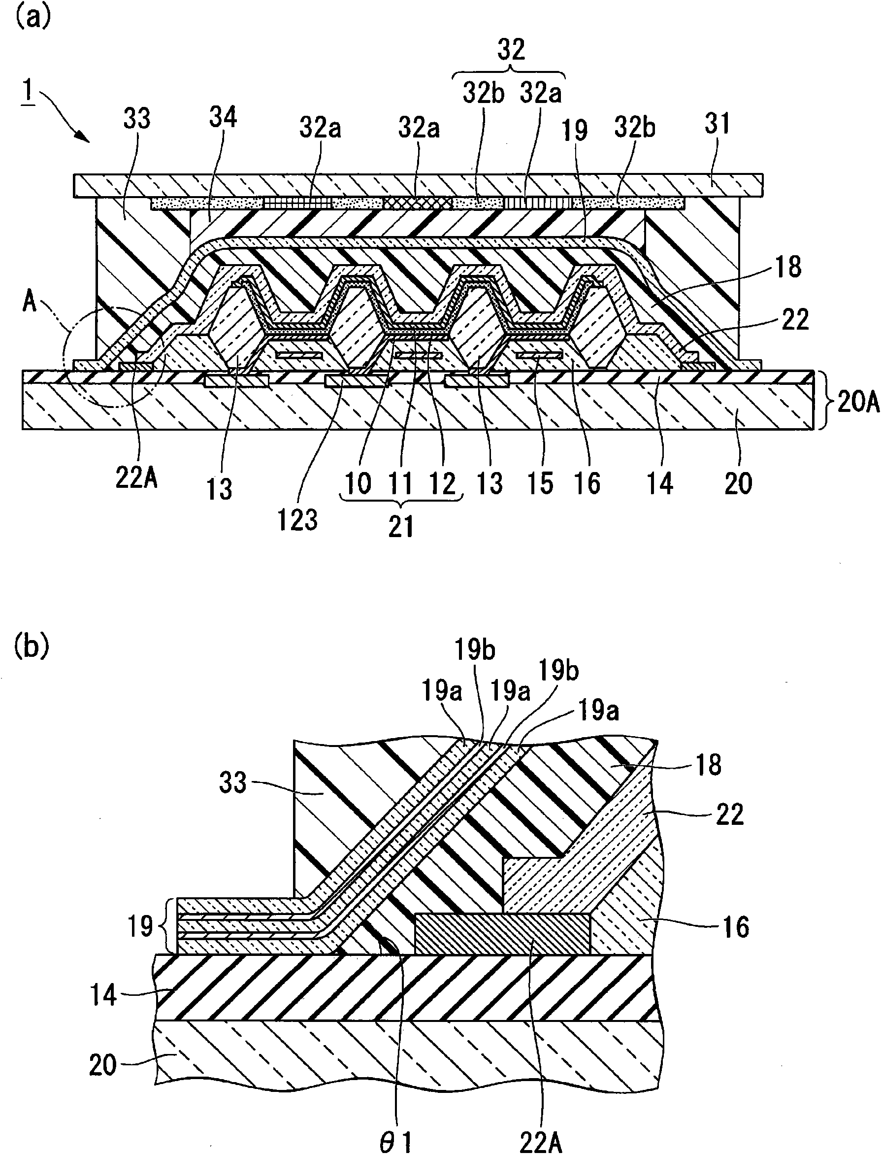
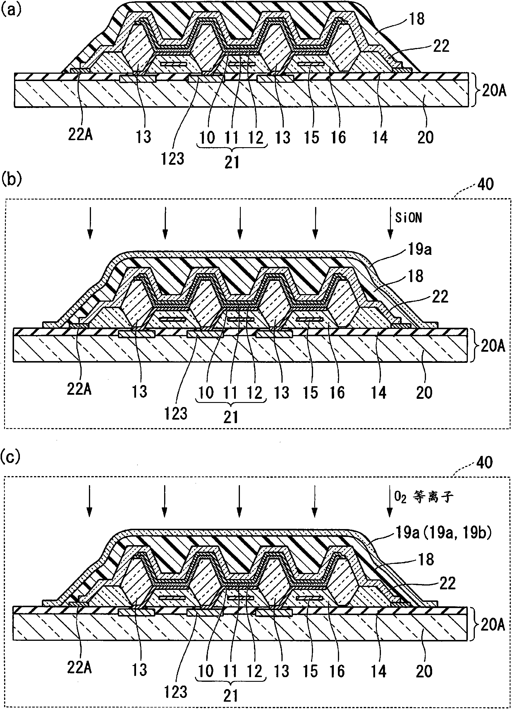
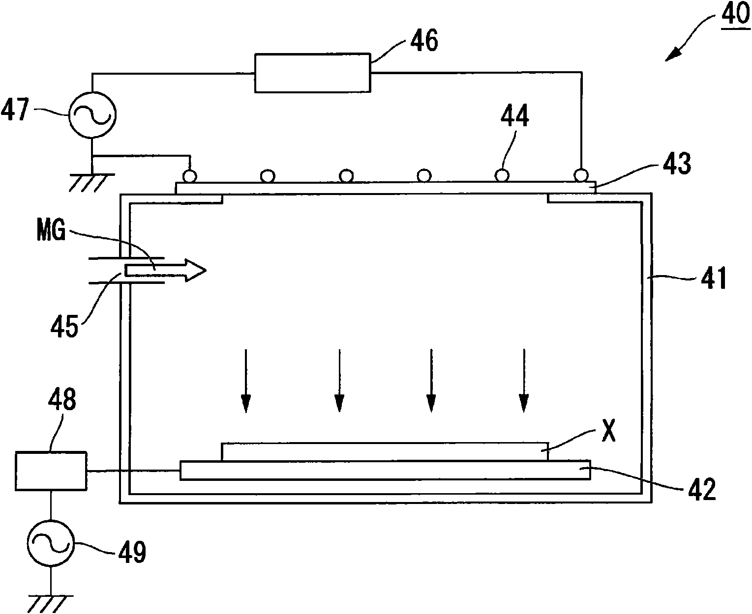
[0047] Below, refer to Figure 1 to Figure 6 , the organic electroluminescent device (organic EL device) according to the first embodiment of the present invention will be described. However, in all the following drawings, the film thicknesses and dimensional ratios of the respective constituent elements are suitably different in order to facilitate viewing of the drawings.
[0048] figure 1 It is a cross-sectional view schematically showing the organic EL device 1 . The organic EL device 1 of the present invention is a so-called "top emission type" organic EL device. Since the top emission method extracts light not from the substrate side where the organic EL element is arranged but from the opposite substrate side, the light-emitting area is not affected by the size of various circuits arranged on the element substrate, and it has the advantage of ensuring a large light-emitting area. Effect. Therefore, luminance can be ensured while suppressing voltage and current, and ...
no. 2 approach
[0145] Figure 7 It is an explanatory diagram of the organic EL device according to the second embodiment of the present invention. The organic EL device of this embodiment is partially shared with the organic EL device of the first embodiment. The difference is that the auxiliary wiring is not provided with a function as a protective layer of the cathode, but an electrode protective layer for protecting the cathode is provided. Therefore, the same reference numerals are assigned to the same components in this embodiment as those in the first embodiment, and detailed description thereof will be omitted.
[0146] like Figure 7 As shown in (a), an auxiliary cathode wiring 24 for supplying electricity to the auxiliary cathode 11 and the cathode wiring 22A is provided at the end of the cathode 11, and covers the entire surface of the cathode 11, the cathode wiring 22A, and the auxiliary cathode wiring 24. An electrode protection layer 17 is formed. With this electrode protect...
Embodiment
[0159] Embodiments of the present invention will be described below. In this example, in order to confirm the effect of the invention, a test body for evaluation which is a substitute of an organic EL device was prepared and evaluated.
[0160] In the test body used in this example, a magnesium film (Mg film) was formed on a glass support substrate, and a thin-film sealing layer composed of an electrode protective layer (SiON) / organic buffer layer / gas barrier layer was formed to cover the Mg film. Furthermore, a glass counter substrate is bonded on the thin film sealing layer. The electrode protection layer is formed so as to be in contact with the supporting substrate and has a structure to seal the Mg film. Furthermore, it is formed so that the electrode protective layer is in contact with the gas barrier layer, and has a structure that seals the organic buffer layer.
[0161] In the test body used, the thicknesses of the respective components were set to Mg film: 50 nm, e...
PUM
 Abstract
Description
Claims
Application Information
 - R&D
- Intellectual Property
- Life Sciences
- Materials
- Tech Scout
- Unparalleled Data Quality
- Higher Quality Content
- 60% Fewer Hallucinations
Browse by: Latest US Patents, China's latest patents, Technical Efficacy Thesaurus, Application Domain, Technology Topic, Popular Technical Reports.
© 2025 PatSnap. All rights reserved.Legal|Privacy policy|Modern Slavery Act Transparency Statement|Sitemap|About US| Contact US: help@patsnap.com


