Chip fuse and process for producing the same

A fuse and chip technology, which is applied in the manufacture of fuses, electrical components, circuits, etc., can solve the problems of not disclosing the heat release device or method of fuse components, and not conducting specific research, etc., and achieves good thickness uniformity and good precision Effect

Active Publication Date: 2010-01-27
KAMAYA ELECTRIC
View PDF2 Cites 2 Cited by
  • Summary
  • Abstract
  • Description
  • Claims
  • Application Information

AI Technical Summary

Problems solved by technology

[0005] However, in Patent Document 2, there is no specific study on the material or heat transfer area of ​​the components around the fuse ele

Method used


Image

  • Chip fuse and process for producing the same
  • Chip fuse and process for producing the same
  • Chip fuse and process for producing the same

Examples


Embodiment Construction

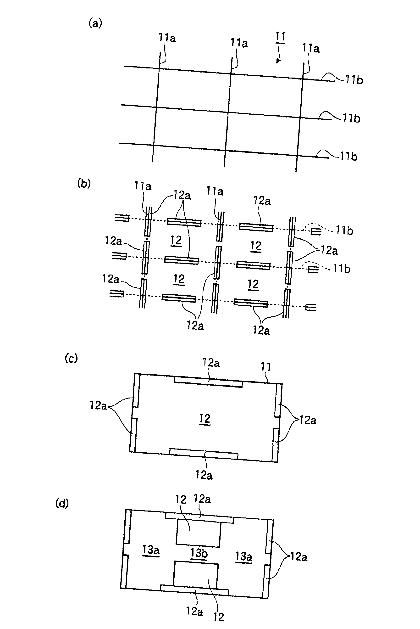
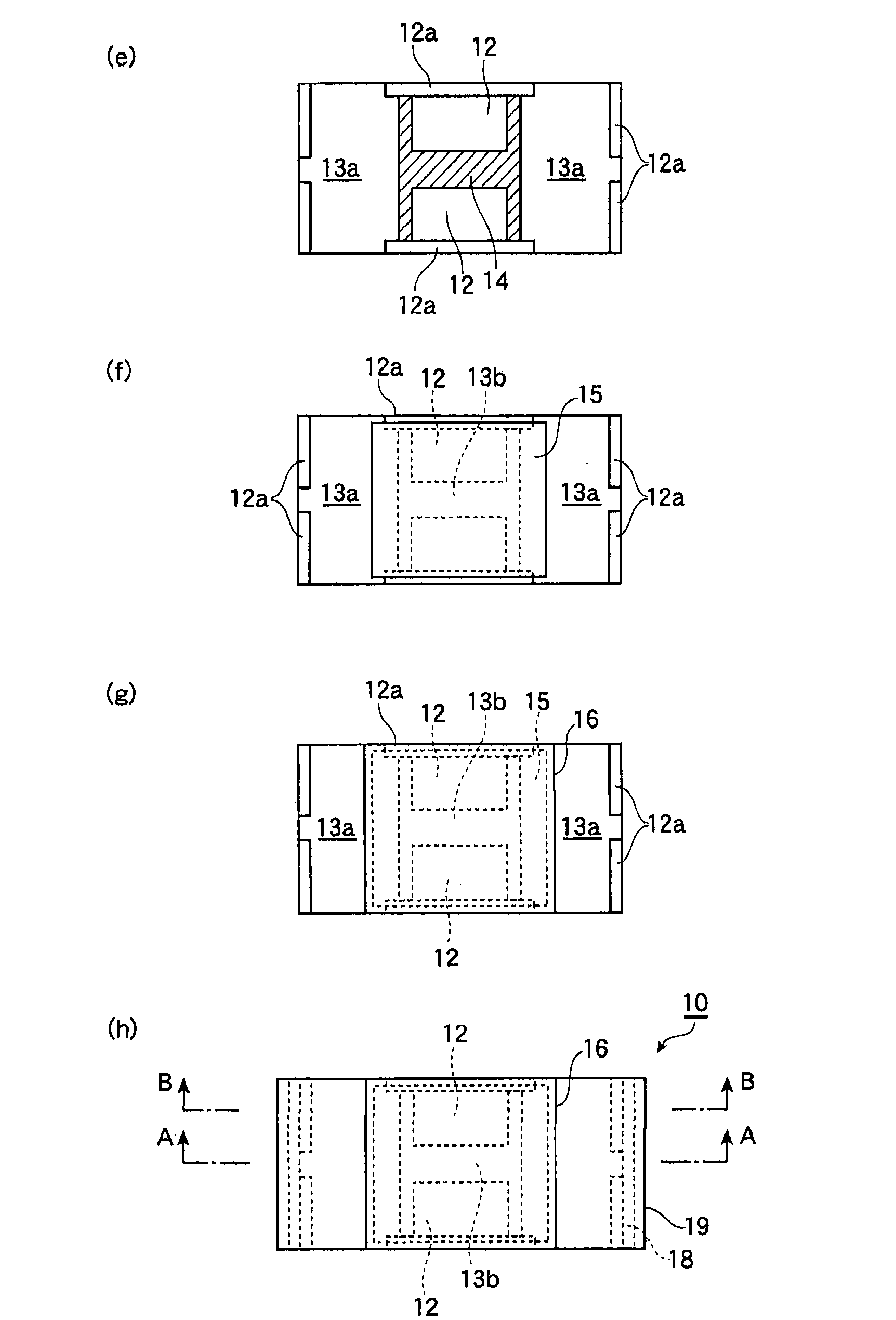
[0033] Hereinafter, an embodiment of the present invention will be described with reference to the drawings, but the present invention is not limited thereto.

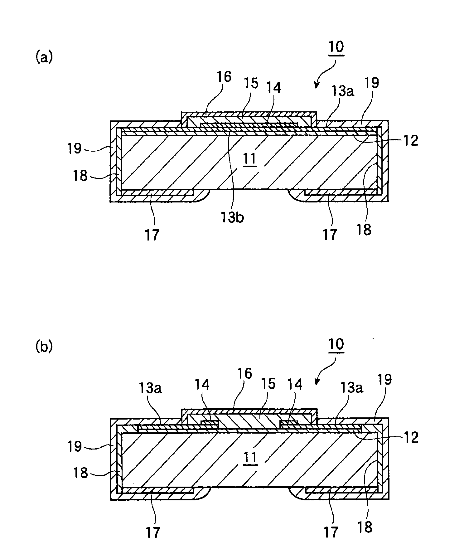
[0034] figure 1 (a)~(d) and figure 2 (e) to (h) are plan views showing the steps of manufacturing the chip fuse 10 of the present invention, image 3 (a) is along figure 2 The sectional view of the chip fuse 10 of the A-A line of (h), image 3 (b) is along figure 2 (h) Cross-sectional view of the chip fuse 10 of the B-B line.

[0035] In the chip fuse 10, a first heat storage layer 12 made of a film material with low thermal conductivity is formed on an insulating substrate 11, and a fuse film 13 is arranged on the first heat storage layer 12. The fuse film 13 There are surface electrode portions 13a arranged at both ends and a fuse element portion 13b formed with a relatively narrow width so as to connect the surface electrode portions 13a at both ends, and a portion of the surface electrode portion 13a and th...


PUM


Abstract

A chip fuse that not restricted in the degree of freedom of fusing characteristics, realizes prevention of shortening of fusing time at large magnification with respect to rated current and attainment of shortening of fusing time at small magnification with respect to rated current. A chip fuse (10) has a first heat storage layer (12) of film material with low thermal conductivity superimposed onan insulating substrate (11) and has a fuse film (13) superimposed on the first heat storage layer (12) so as to avoid contact with the insulating substrate (11). The fuse film (13) has a fuse element part (13b) interposed between surface electrode parts (13a) disposed at both edges thereof. A second heat storage layer (15) of film material with low thermal conductivity is superimposed on the fuse element part (13b). The first heat storage layer (12) is thicker than the second heat storage layer (15). The first heat storage layer (12) and second heat storage layer (15) are those produced froma sheet material of B-stage state containing a photosensitive group.

Description

technical field [0001] The present invention relates to a chip fuse and a manufacturing method thereof, and more particularly to a chip fuse in which an upper layer and a lower layer of a fuse element portion are formed of a film having low thermal conductivity, and a manufacturing method thereof. Background technique [0002] Regarding chip fuses, there is, for example, the technology described in Patent Document 1 as an already disclosed technology. Wherein a silicone resin film is formed on the upper surface of the inorganic substrate, a fuse film is formed on the silicone resin film, and a protective film is formed from silicone resin on the fuse film, the thickness of the silicone resin film on the upper surface of the substrate is , exemplifying 10 μm. [0003] It has been described in Patent Document 1 that the use of silicone resin prevents melting and burning of the solder at the connection part with the printed wiring board, but the degree of freedom of the fusing...

Claims


Application Information

Patent Timeline
IPC IPC(8): H01H85/045H01H69/02H01H85/0445H01H85/046H01H85/10H01H85/17
CPCH01H85/006H01H85/0411H01H2085/0283H01H85/0065H01H2085/0414H01H85/10H01H85/046H01H69/02H01H85/00
Inventor 山岸克哉清野英树佐藤仁
Owner KAMAYA ELECTRIC
Why Eureka
Try Eureka