Supercharge Your Innovation With Domain-Expert AI Agents!

Method for manufacturing semiconductor structure

A manufacturing method and semiconductor technology, applied in semiconductor/solid-state device manufacturing, electrical components, circuits, etc., can solve problems such as device damage, achieve the effects of improving efficiency, avoiding unstable factors in the process chamber, and protecting from damage

Inactive Publication Date: 2012-10-10
SEMICONDUCTOR MANUFACTURING INTERNATIONAL (BEIJING) CORP
View PDF6 Cites 0 Cited by
  • Summary
  • Abstract
  • Description
  • Claims
  • Application Information

AI Technical Summary

Problems solved by technology

[0009] The invention provides a method for manufacturing a semiconductor structure to solve the problem of plasma damage to devices on a substrate in the process of forming a pre-metal dielectric layer

Method used


Image

  • Method for manufacturing semiconductor structure
  • Method for manufacturing semiconductor structure
  • Method for manufacturing semiconductor structure

Examples


Embodiment Construction

[0028] The specific embodiments of the present invention will be described in detail below in conjunction with the accompanying drawings.

[0029] In the following description, numerous specific details are set forth in order to provide a thorough understanding of the present invention. However, the present invention can be implemented in many other ways different from those described here, and those skilled in the art can make similar extensions without violating the connotation of the present invention, so the present invention is not limited by the specific implementations disclosed below.

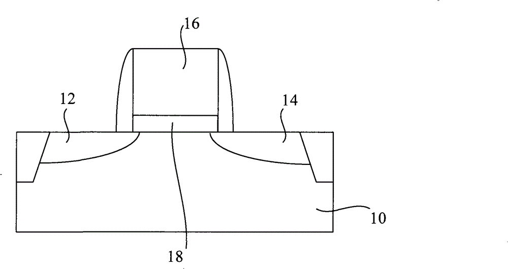
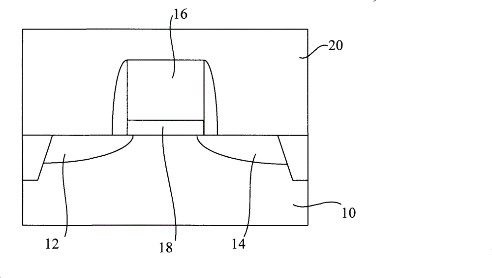
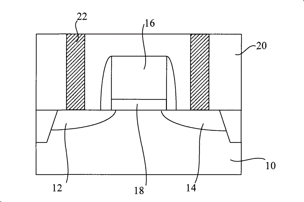
[0030] Secondly, the present invention is described in detail using schematic diagrams. When describing the embodiments of the present invention in detail, for the convenience of explanation, the cross-sectional view showing the device structure will not be partially enlarged according to the general scale, and the schematic diagram is only an example, and it should not be limited here. ...


PUM


Abstract

The invention discloses a method for manufacturing a semiconductor structure, which comprises the steps of: providing a substrate provided with a semiconductor device; and forming a dielectric layer on the semiconductor device, wherein the step of forming the dielectric layer at least comprises two stages of: the first stage, forming a protective layer covering the semiconductor device; and the second stage, executing a plasma deposition process, and depositing a dielectric layer on the protective layer. The method can reduce or eliminate the damage to the semiconductor device of the substrate in the step of forming the dielectric layer.

Description

technical field [0001] The invention relates to the technical field of semiconductor manufacturing, in particular to a method for manufacturing a semiconductor structure. Background technique [0002] In the manufacturing process of semiconductor integrated circuits, devices are formed on a substrate through a series of processes such as photolithography, etching, deposition and planarization, and a metal interconnection structure connecting each device is formed on the devices. The device and the metal interconnection structure are connected through contact plugs in the pre-metal dielectric layer. Wherein, the pre-metal dielectric layer covers the device and is used as an insulating layer between the device and the metal interconnection structure, and is generally formed by a chemical vapor deposition process. [0003] Figure 1 to Figure 3 It is a schematic cross-sectional view of forming a pre-metal dielectric layer on a device and forming a connection plug in the pre-me...

Claims


Application Information

Patent Timeline
Patent Type & Authority Patents(China)
IPC IPC(8): H01L21/31H01L21/316H01L21/314H01L21/768
Inventor 李敏郑春生张子莹
Owner SEMICONDUCTOR MANUFACTURING INTERNATIONAL (BEIJING) CORP
Features
  • R&D
  • Intellectual Property
  • Life Sciences
  • Materials
  • Tech Scout
  • Unparalleled Data Quality
  • Higher Quality Content
  • 60% Fewer Hallucinations
Learn More