Power semiconductor module

一种功率半导体、层叠体的技术,应用在半导体器件、半导体/固态器件零部件、电固体器件等方向,能够解决没有公开影响等问题,达到抑制破裂、消除脆性、减少变形的效果

Inactive Publication Date: 2012-12-05
TOYOTA JIDOSHA KK +1
View PDF7 Cites 0 Cited by
  • Summary
  • Abstract
  • Description
  • Claims
  • Application Information

AI Technical Summary

Problems solved by technology

[0021] However, in this document, only the strength of the insulator is evaluated, and the evaluation is not performed in the state of a module in which other members such as power semiconductors and heat sinks are welded together.
Therefore, the effect of the Cu / SiNx / Cu laminate on the weakest solder joint is not disclosed

Method used


Image

  • Power semiconductor module
  • Power semiconductor module
  • Power semiconductor module

Examples


preparation example Construction

[0136] The method for producing CuAlMn alloy particles is not particularly limited, and known methods for producing alloy particles can be appropriately used. An example of the production method is given below, but is not limited thereto.

[0137] First, Cu, Al, and Mn were melted in a high-frequency melting furnace under an Ar atmosphere to produce a CuAlMn alloy ingot as a precursor. The above-mentioned additional elements may be added to the ingot as needed. Next, the obtained ingot is pulverized by a powder production technique such as an atomization method to obtain CuAlMn alloy particles. The powdered CuAlMn alloy particles are plated with Ni and Au on the surface of the particles by a dropping method or the like. By adjusting the film thickness of the plating layer on the surface of the particles, the dispersibility of the CuAlMn particles in Bi—CuAlMn can be improved. The preferable film thickness of this plating layer is 0.01-3 micrometers.

[0138] When the insul...

Embodiment 1

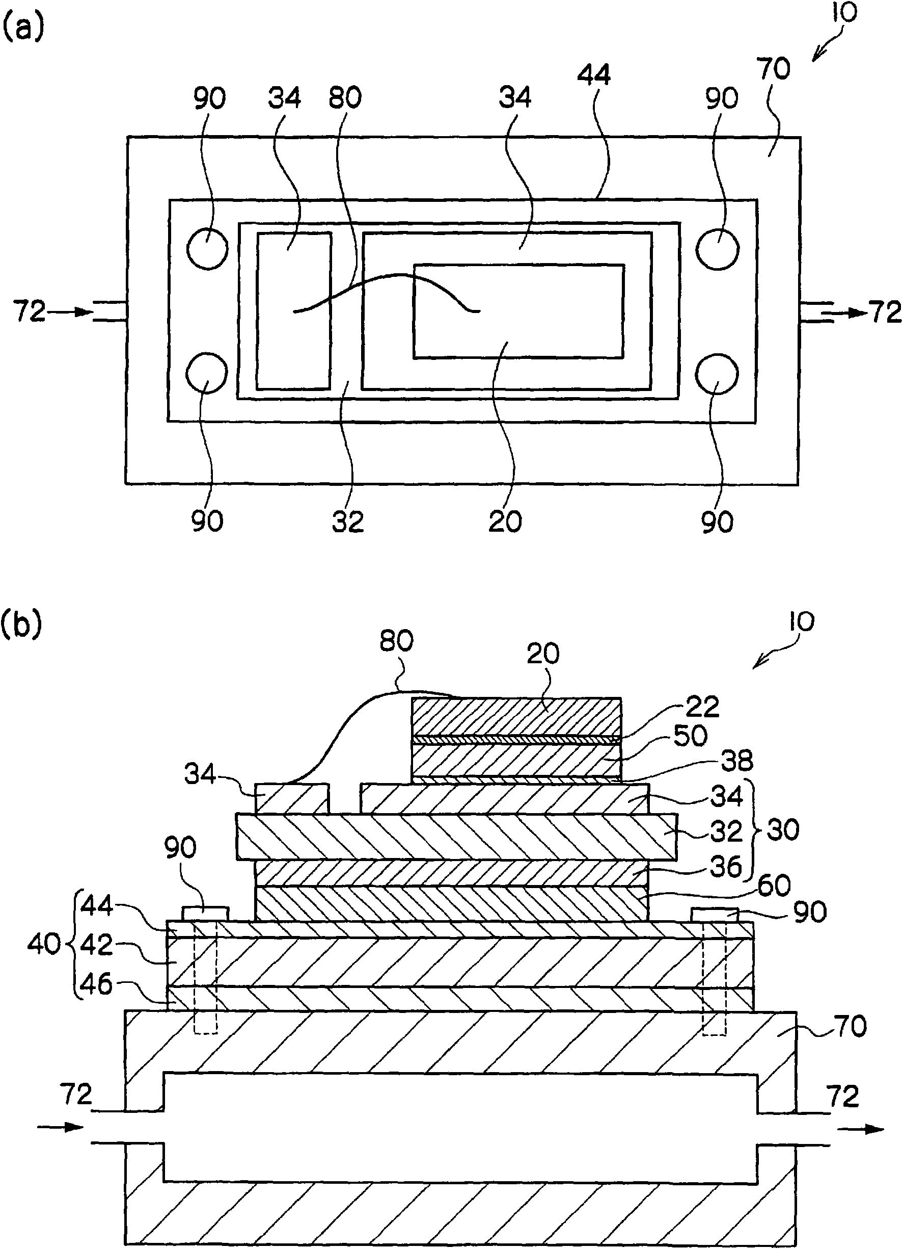
[0290] figure 1 The structure of the power semiconductor module of this embodiment is shown in .

[0291]

[0292] A 12 mm×9 mm power semiconductor element 20 using SiC (thermal expansion coefficient: 3 ppm / ° C.) was prepared, and a Ni layer 22 was formed on the outermost surface by sputtering. An Au layer (not shown) is formed on the surface of the Ni layer 22 by sputtering.

[0293]

[0294] As the insulating portion 30 , a laminate of Cu layer 34 / SiNx layer 32 / Cu layer 36 was fabricated.

[0295] First, SiNx with a thickness of 0.32 mm was prepared, and Cu layers 34 and 36 with a thickness of 0.05 mm were attached to both surfaces of the SiNx by brazing to produce a laminate-1.

[0296] In the same manner, but changing the thickness of the Cu layers 34 and 36 to 0.1 mm, 0.15 mm, and 0.3 mm, laminates-2, -3, and -4 were produced. In addition, the thickness of the Cu layer was made equal on both sides of SiNx.

[0297] In the laminated bodies-1 to 4, the Ni layer 38...

Embodiment 2

[0323] made as Figure 8 Shown is an evaluation test body-1 in which a power semiconductor element and an insulating part are joined with a Bi-based solder material.

[0324]

[0325] A 12 mm×9 mm power semiconductor element 20 using SiC (thermal expansion coefficient: 3 ppm / ° C.) was prepared, and a Cu layer 22 was formed on the outermost surface by sputtering.

[0326]

[0327] Insulator laminate-2 (thickness of Cu layer: 0.1 mm) of Example 1 was prepared.

[0328]

[0329] The Bi simple substance is cut into a thickness of 150 to 200 μm. The oxide film covering the surface of the excised Bi simple substance layer was removed by grinding and acid washing.

[0330] The Cu layer 22 of the power semiconductor element 20 prepared above and the Cu layer 34 of the insulating part 30 were arranged facing each other, and a Bi simple substance layer was interposed therebetween. 2 / N 2 The bonding was performed at a bonding temperature of 320° C. by a reflow method in a redu...


PUM


Abstract

Provided is a power semiconductor module in which two components are bonded by a Bi based solder material. A Cu layer is provided on the surfaces thereof to be bonded by the Bi based solder material on the two-component. Two components, i.e., the components to be bonded, are a combination of a semiconductor element and an insulating part, or a combination of an insulating part and a radiator plate. The insulating part is composed of a Cu / SiNx / Cu laminated body.

Description

technical field [0001] The invention relates to power semiconductor modules. Background technique [0002] In a power semiconductor module, an insulator is usually provided on the power semiconductor so as to electrically insulate the power semiconductor from the current-carrying part. The power semiconductor and the insulator are joined with solder or the like. [0003] In addition, in the power semiconductor module, in order to efficiently dissipate heat generated by the semiconductor element or temporarily dissipate the heat, a heat dissipation plate is provided, and the heat dissipation plate and the above-mentioned insulator are bonded by solder. Therefore, in a power semiconductor module, solder is usually used to join two places: between the semiconductor element and the insulator, and between the insulator and the heat sink. [0004] Since a large current flows through the power semiconductor element, the power semiconductor module generates power loss (constant lo...

Claims


Application Information

Patent Timeline
Patent Type & Authority Patents(China)
IPC IPC(8): H01L25/07H01L23/36H01L25/18
CPCH01L2924/01015H01L2224/83805H01L2924/01032H01L2224/45124H01L2224/29113H01L2924/01082H01L2924/0105H01L2924/01004H01L2924/01025H01L2924/01018H01L2924/01002H01L24/32H01L2924/01019H01L2924/01322H01L2924/01029H01L2224/29111H01L23/3735H01L2924/0132H01L2924/01027H01L2924/01028H01L2224/48472H01L2224/48091H01L2924/01013H01L2924/014H01L2224/32225H01L2924/0103H01L2224/83447H01L24/45H01L24/33H01L23/473H01L2924/01047H01L2924/0133H01L2924/01079H01L24/48H01L2224/838H01L2224/48227H01L24/83H01L2924/01033H01L2924/01005H01L2924/1579H01L24/29H01L2924/01006H01L25/072H01L2924/01078H01L2924/01042H01L2924/01014H01L2224/73265H01L2924/01051H01L2924/351H01L2924/00011H01L24/73H01L2224/2612H01L2924/00014H01L2924/00H01L2924/00012H01L2924/01083H01L2924/3512H01L2924/00015H01L2224/83205
Inventor 八木雄二山田靖中川郁朗渥美贵司白井干夫大沼郁雄石田清仁高久佳和
Owner TOYOTA JIDOSHA KK
Why Eureka
Try Eureka