Semiconductor wafer film thickness detecting device on basis of infrared optical interference method

A technology of infrared optics and detection devices, which is applied in the direction of optical devices, measuring devices, semiconductor/solid-state device testing/measurement, etc., can solve the problems of not being easy to detect concentric circles, wafer detection, troublesome layout, etc., to achieve signal Processing and automatic detection, improving product quality, and good stability

Active Publication Date: 2013-04-17
THE 45TH RES INST OF CETC
View PDF0 Cites 1 Cited by
  • Summary
  • Abstract
  • Description
  • Claims
  • Application Information

AI Technical Summary

Problems solved by technology

However, the existing film thickness detection devices have the following disadvantages: 1. A fixed light source is used in the mechanical structure, and then the film table is moved in the X-Y direction to determine the detection point. The disadvantage is that it is not easy to detect the points on the concentric circles, so it cannot It is better to detect the wafer after adopting regional pressure control, and the layout is more troublesome
2. The data detection operation is realized by hardware circuits such as multipliers and low-pass filters, with low precision and poor flexibility

Method used


Image

  • Semiconductor wafer film thickness detecting device on basis of infrared optical interference method
  • Semiconductor wafer film thickness detecting device on basis of infrared optical interference method
  • Semiconductor wafer film thickness detecting device on basis of infrared optical interference method

Examples


Embodiment Construction

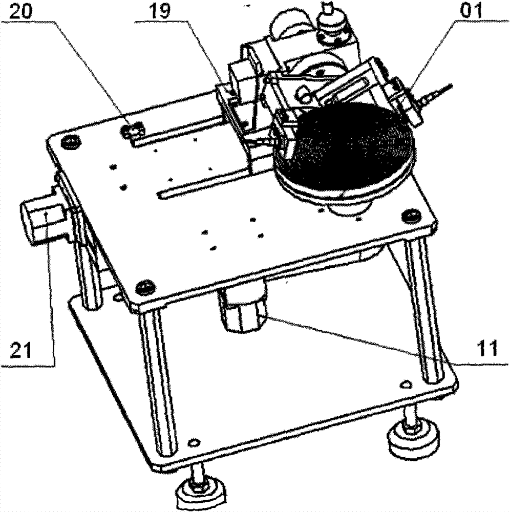
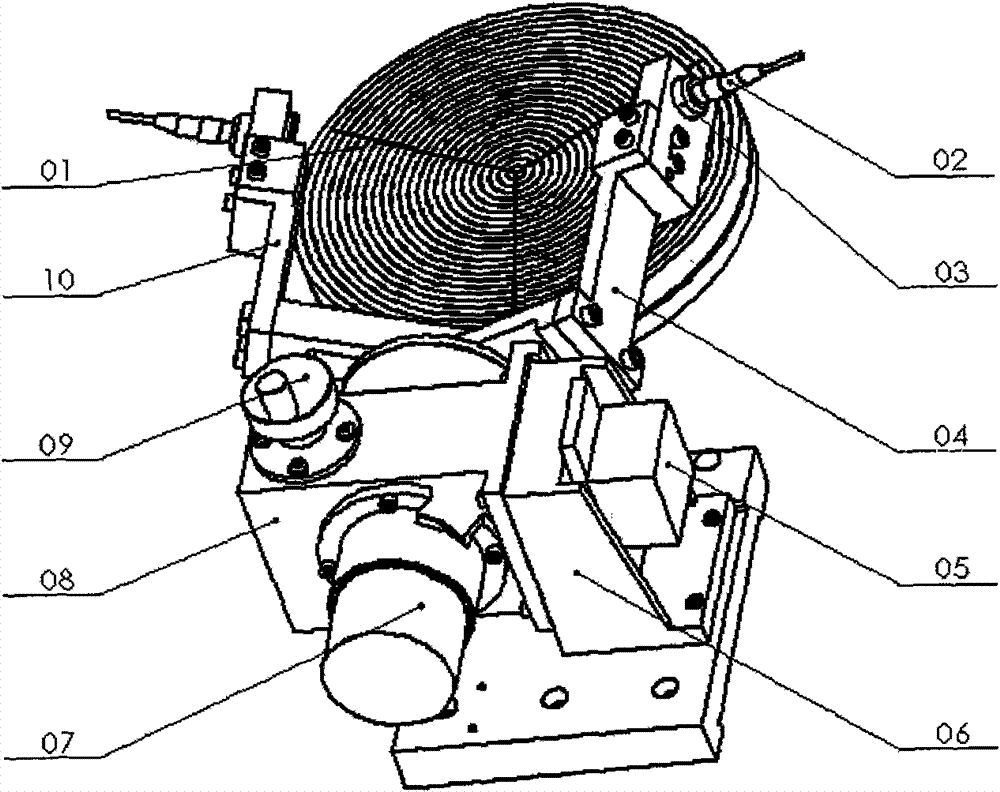
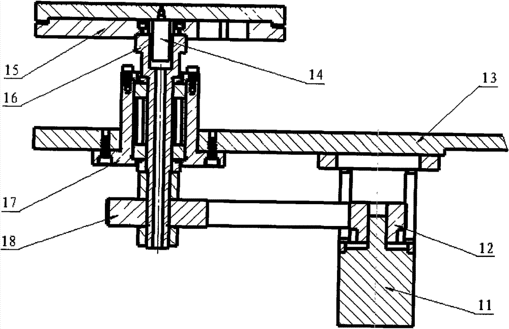
[0031] The structure of the device of the present invention is mainly composed of three parts: the carrying and rotating mechanism of the wafer, the adjustment and moving mechanism of the laser, and the vacuum adsorption gas path of the wafer. The structure of the device is as follows: figure 1 shown.

[0032] Based on the principle of thin film interference of light, such as Figure 10 . The light intensity after interference is

[0033] E = E 1 + E 2 + 2 E 1 E 2 cos ( 4 n 2 π d cos θ λ )

[0034] The film thickness d can be...


PUM


Abstract

The invention provides a semiconductor wafer film thickness detecting device on the basis of an infrared optical interference method and relates to the technical field of chemical-mechanical polishing devices for a semiconductor wafer. The device comprises a wafer bearing and moving mechanism, a laser assembly and a data detecting and controlling circuit and is characterized in that the laser assembly is a movable laser assembly and the wafer bearing and moving mechanism is a wafer bearing and rotating mechanism. By adopting the device, multi-point detection on the surface of the wafer can becarried out, thus knowing the thickness and distribution condition of a wafer surface film layer so as to ensure the process parameters of a next polishing process, thus perfecting the polishing process and increasing the product quality. The device is especially suitable for the chemical-mechanical polishing device for the semiconductor wafer.

Description

technical field [0001] The invention relates to the technical field of an optical interference method film thickness detection device on chemical mechanical polishing equipment for semiconductor wafers. Background technique [0002] In semiconductor device processing, it is necessary to perform a CMP operation to remove processing defects to obtain high planarity. Before polishing, it is necessary to have a certain understanding of the condition of the film layer on the surface of the wafer to determine the polishing parameters; after polishing, it is necessary to understand the polishing status to determine the next polishing process. However, the existing film thickness detection devices have the following disadvantages: 1. A fixed light source is used in the mechanical structure, and then the film table is moved in the X-Y direction to determine the detection point. The disadvantage is that it is not easy to detect the points on the concentric circles, so it cannot It is...

Claims


Application Information

Patent Timeline
Patent Type & Authority Patents(China)
IPC IPC(8): G01B11/06H01L21/66
Inventor 吴旭陈波王东辉柳滨
Owner THE 45TH RES INST OF CETC
Why Eureka
Try Eureka