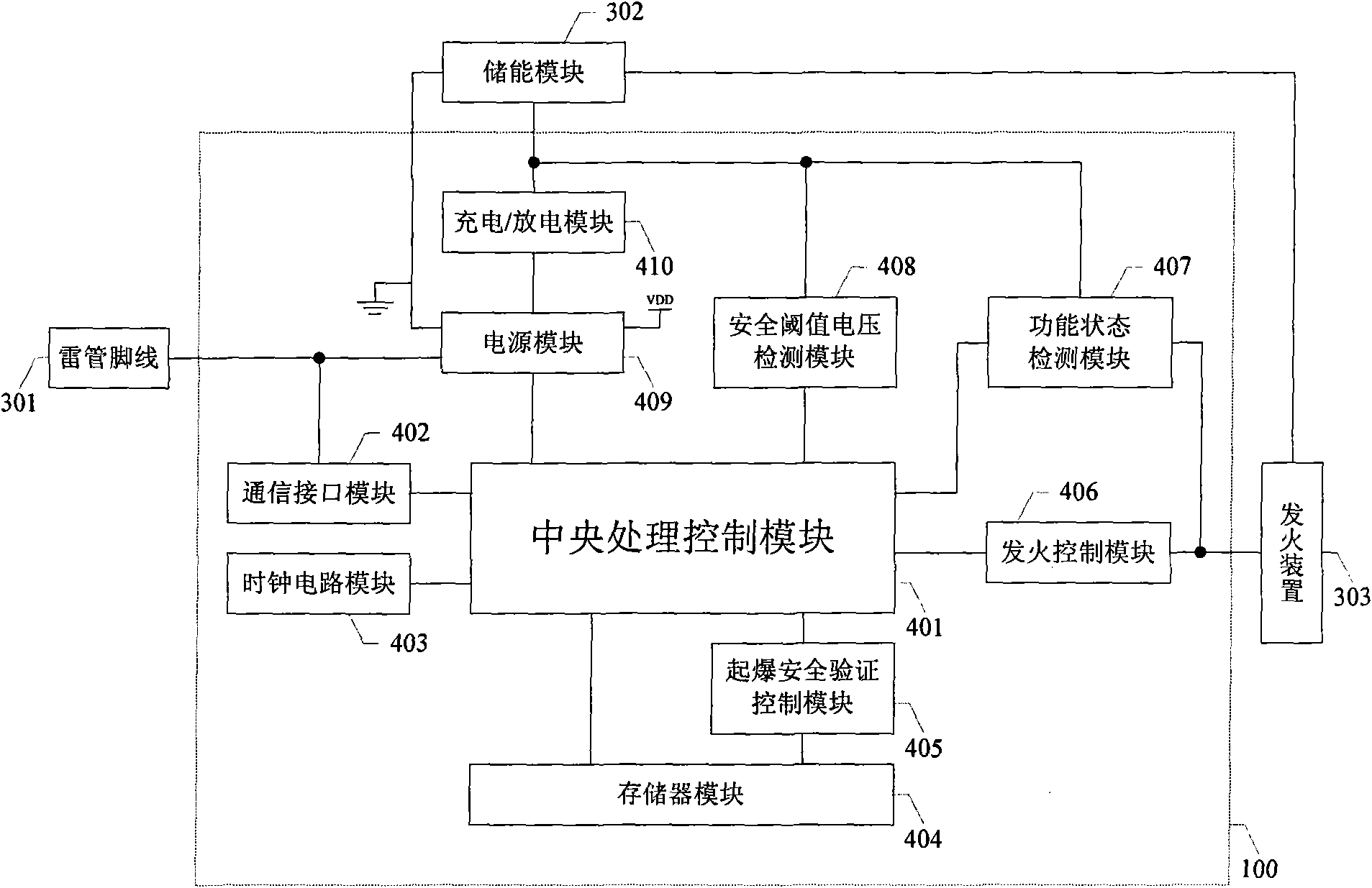
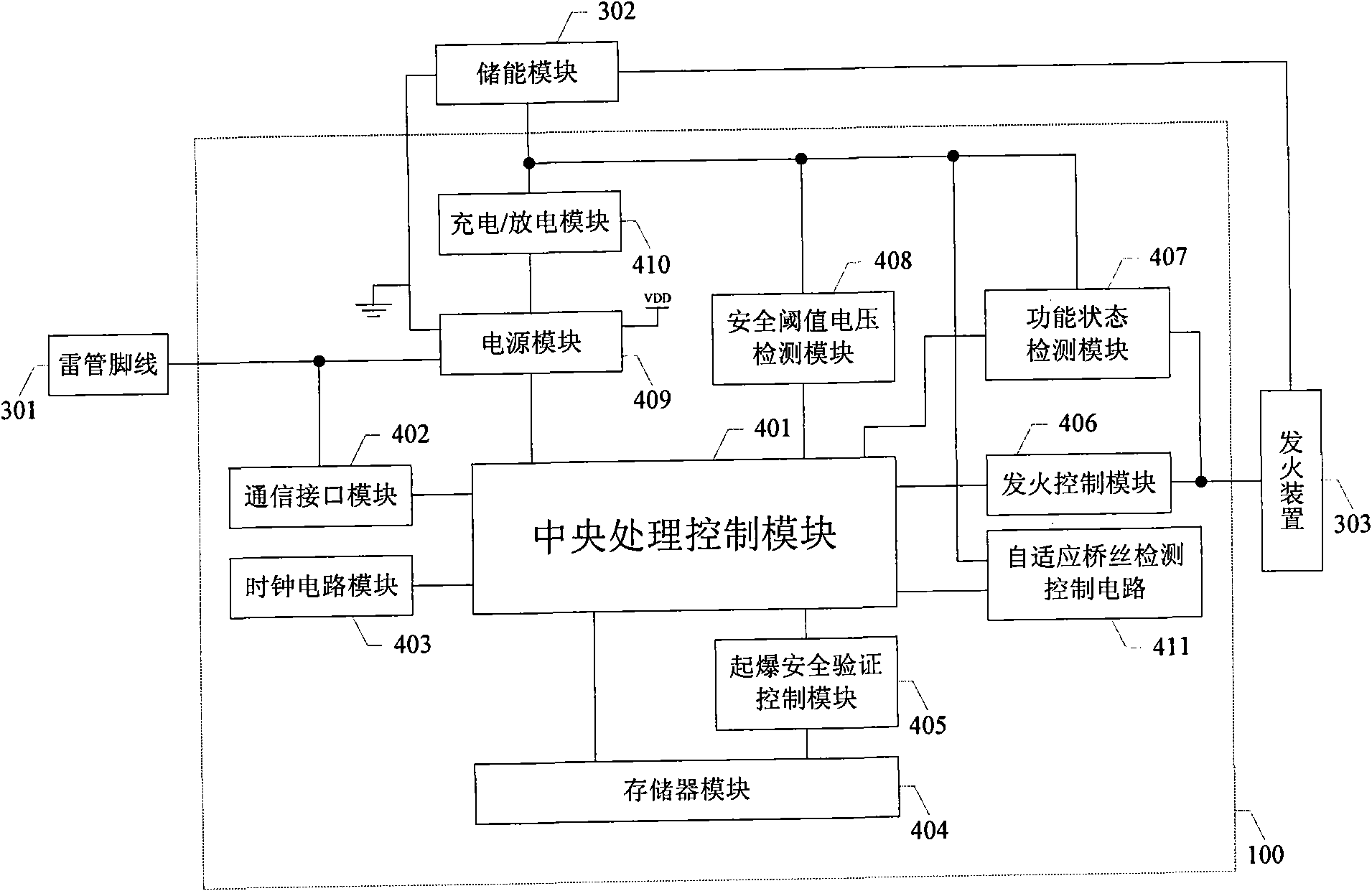
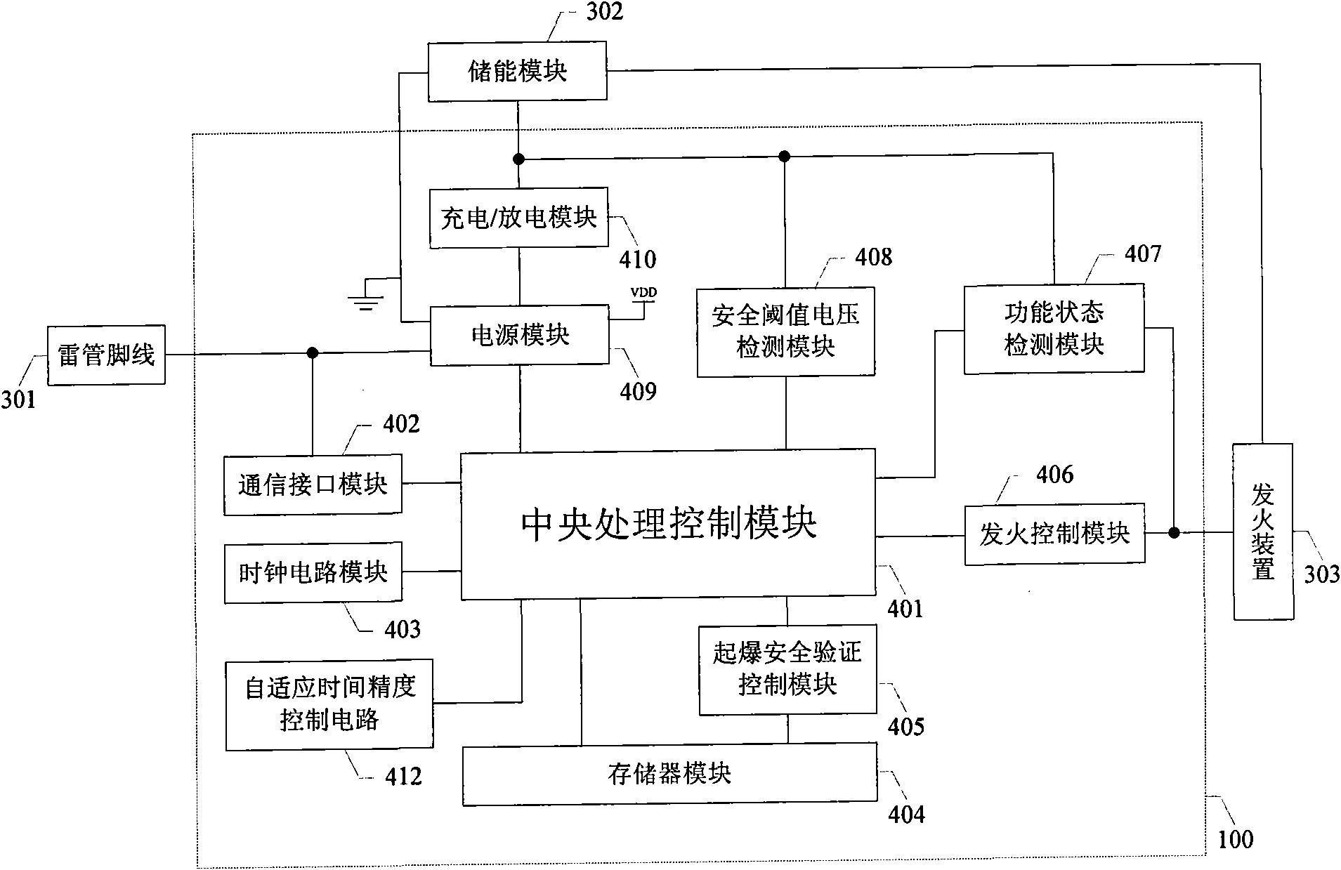
[0046] Such as figure 1 As shown, the present invention provides a digital electronic detonator control chip 100, which includes a central processing control module 401, a communication interface module 402, a clock circuit module 403, a memory module 404, a detonation safety verification control module 405, an ignition control module 406, and functional status A detection module 407, a safety threshold voltage detection module 408, a power supply module 409, and a charging/discharging module 410.
[0047] First of all, the digital electronic detonator control chip is provided by the detonator pin 301 with a DC voltage, such as a DC 12V voltage, or using carrier wave as the power supply input, so that the detonator pin 301 is directly connected to the power module 409 and passes through the inside of the power module. The bridge rectifier is connected to the charging/discharging module 410 on the one hand to charge the energy storage module 302. The energy storage module 302 contains two capacitors. One capacitor is responsible for the internal logic power supply of the chip, referred to as the working capacitor, and the other capacitor is the detonation The power supply of the timing ignition device, referred to as the detonating capacitor, on the other hand, is also converted into the power supply for the internal logic of the chip through the DC-DC voltage, which supplies power to all the units in the chip that need power. When the detonator pin 301 does not provide a power input state, The power supply inside the chip is taken from the working capacitor of the energy storage module 302; after the internal power supply reaches a certain voltage, the clock circuit module of the chip starts to work, and the central processing control module 401 starts power-on initialization. After the initialization is completed, the digital electronic detonator control chip is in the standby state , Ready to receive commands from the detonator or programmer, and perform related operations.
[0048] Receiving commands from the detonator or programmer is implemented through the communication interface module 402. One end of the communication interface module 402 is connected to the detonator pin 301 and the power supply module 409, and the other end is connected to the central processing control module 401 to realize the detonator /Programmer and chip internal control data communication.
[0049] When the detonator/programmer prepares for online testing of the digital electronic detonator, when the detonator/programmer issues a charge check command, the command is transmitted to the central processing control module 401 through the detonator pin line 301 and the communication interface module 402. The processing control module 401 sends a control signal to the function state inspection module 407 and the charge/discharge/discharge module 410 to check the on-off condition of the charging circuit, and mainly detects whether the detonating capacitor can be reliably charged.
[0050] When the detonator/programmer prepares for online testing of the digital electronic detonator, when the detonator/programmer issues a discharge inspection command, the command is transmitted to the central processing control module 401 through the detonator pin line 301 and the communication interface module 402. The processing control module 401 sends a control signal to the function state inspection module 407 and the charge/discharge/discharge module 410 to check the on and off of the discharge circuit, and mainly detects whether the detonating capacitor can be reliably discharged.
[0051] When the detonator/programmer prepares for online testing of the digital electronic detonator, when the detonator/programmer issues a fire check command, the command is transmitted to the central processing control module 401 through the detonator pin line 301 and the communication interface module 402. The processing control module 401 sends a control signal to the functional status check module 407 and the ignition control module 406 to check the on and off of the ignition circuit, especially the on and off of the ignition device's bridge wire, to ensure reliable ignition and detonation when the detonation command is issued.
[0052] When the programmer is ready to program the digital electronic detonator, the programmer issues a set detonation delay command to program the digital electronic detonator. The command is transmitted to the central processing control module 401 through the detonator pin line 301 and the communication interface module 402. The central processing control module 401 receives the time information of the initiation delay, sends a control signal to the memory module 404, and stores the delay time information in the memory module 404.
[0053] When the detonator is ready to perform detonation verification on the digital electronic detonator, the detonator issues a set detonation verification command, which is transmitted to the central processing control module 401 through the detonator pin line 301 and the communication interface module 402, and the central processing control module 401 issues control The signal is sent to the detonation safety verification control module 405 and the memory module 404. The detonation safety verification module 405 compares the detonation password received from the detonator with the detonation password transmitted from the memory module 404. If the passwords are consistent, the central processing control module 401 sends control Signal, set the detonation flag inside the memory module to be valid, otherwise an error message will be returned to the detonator.
[0054] When the detonator is ready to detonate the digital electronic detonator, the detonating capacitor of the digital electronic detonator must be charged before detonation. When the detonation charge command is initiated under the detonator, the command is transmitted to the detonator pin 301 and the communication interface module 402. The central processing control module 401, the central processing control module 401 sends a control signal to control the charging/discharging module 410 to charge the detonating capacitor.
[0055] After the blasting system is tested before detonation and everything is ok, the detonator initiates a detonation command, which is transmitted to the central processing control module 401 through the detonator pin 301 and the communication interface module 402, and the central processing control module 401 sends a control signal to the fire The control module 406 turns on the ignition circuit, the detonating capacitor discharges the ignition circuit, a large current flows through the ignition bridge wire, the bridge wire generates heat and ignites, and the digital electronic detonator is blasted.
[0056] In addition, during the working process of the digital electronic detonator chip, the safety threshold voltage detection module 408 always monitors the voltage of the detonating capacitor. If it exceeds the safety threshold voltage, it sends information to the central processing control module 401, and the central processing control module 401 controls charging and discharging. The discharge module 410 discharges the detonating capacitor to ensure the safety of the digital electronic detonator.
[0057] In short, the digital electronic detonator chip can be programmed to set the detonation delay online, and can be detected online, and can detonate only after passing the detonation safety verification, which is convenient for centralized supervision and control, and is suitable for my country's regulatory environment and requirements.
[0058] Such as figure 2 What is shown is an optimized embodiment of the digital electronic detonator control chip 100 provided by the present invention. figure 2 in figure 1 Based on this, an adaptive bridge wire detection control circuit 411 is added.
[0059] The digital electronic detonator control chip 100 includes a central processing control module 401, a communication interface module 402, a clock circuit module 403, a memory module 404, a detonation safety verification control module 405, an ignition control module 406, a functional state detection module 407, and a safety threshold Voltage detection module 408, power supply module 409, charging/discharging module 410, adaptive bridge wire detection control circuit 411.
[0060] with figure 1 Similarly, for the digital electronic detonator control chip, the detonator pin 301 provides DC voltage, or the carrier is used as the power supply input, so that the detonator pin 301 is directly connected to the power module 409, and is rectified by the internal bridge of the power module. It is connected to the charging/discharging module 410 to charge the energy storage module 302. The energy storage module 302 contains two capacitors. One capacitor is responsible for the internal logic power supply of the chip, referred to as the working capacitor, and the other capacitor is the power supply for the ignition device during detonation, referred to as The detonating capacitor, on the other hand, is converted into the power supply for the internal logic of the chip through the DC-DC voltage to supply power to all the units in the chip that need power. When the detonator pin 301 does not provide power input status, the internal power supply of the chip is taken from The working capacitor of the energy storage module 302; after the internal power supply reaches a certain voltage, the chip clock circuit module starts to work, and the central processing control module 401 starts power-on initialization. After the initialization is completed, the digital electronic detonator control chip is in a standby state, ready to receive the detonator or Commands of the programmer to perform related operations.
[0061] In order to improve the consistency of digital electronic detonators, the detonator or programmer sends a system self-check command, which is transmitted to the central processing control module 401 through the detonator pin 301 and the communication interface module 402, and the central processing control module 401 sends a control signal to The adaptive bridge wire detection control circuit 411 and the functional status detection module 407 make the ignition device form a loop. The adaptive bridge wire detection control circuit 411 tests the resistance of the ignition circuit to compare with the equivalent resistance of the designed ignition circuit. The resistance value is automatically compensated to make the equivalent circuit of the ignition circuit close to a constant value, thereby achieving the consistency and reliability of ignition, and indirectly improving the accuracy of blasting delay.
[0062] In addition, figure 2 Other workflows and control relationships and figure 1 same.
[0063] Such as image 3 What is shown is an optimized embodiment of the digital electronic detonator control chip 100 provided by the present invention. image 3 in figure 1 Based on this, an adaptive time accuracy control circuit 412 is added.
[0064] The digital electronic detonator control chip 100 includes a central processing control module 401, a communication interface module 402, a clock circuit module 403, a memory module 404, a detonation safety verification control module 405, an ignition control module 406, a functional state detection module 407, and a safety threshold Voltage detection module 408, power supply module 409, charging/discharging module 410, adaptive time accuracy control circuit 412.
[0065] with figure 1 Similarly, for the digital electronic detonator control chip, the detonator pin 301 provides DC voltage, or the carrier is used as the power supply input, so that the detonator pin 301 is directly connected to the power module 409, and is rectified by the internal bridge of the power module. It is connected to the charging/discharging module 410 to charge the energy storage module 302. The energy storage module 302 contains two capacitors. One capacitor is responsible for the internal logic power supply of the chip, referred to as the working capacitor, and the other capacitor is the power supply for the ignition device during detonation, referred to as The detonating capacitor, on the other hand, is converted into the power supply for the internal logic of the chip through the DC-DC voltage to supply power to all the units in the chip that need power. When the detonator pin 301 does not provide power input status, the internal power supply of the chip is taken from The working capacitor of the energy storage module 302; after the internal power supply reaches a certain voltage, the chip clock circuit module starts to work, and the central processing control module 401 starts power-on initialization. After the initialization is completed, the digital electronic detonator control chip is in a standby state, ready to receive the detonator or Commands of the programmer to perform related operations.
[0066] When the detonator/programmer is ready to calibrate and compensate the delay time of the digital electronic detonator, the detonator/programmer issues a communication check command, which is transmitted to the central processing control module through the detonator pin 301 and the communication interface module 402 401. The central processing control module 401 controls the memory module 404, obtains the ID number of the digital electronic detonator chip, and sends it back to the recovery initiator/programmer. At the same time, the central processing control module 401 records the returned time information and receives the detonation again The controller/programmer issues a communication reply command. The adaptive time accuracy control circuit 412 automatically obtains the communication and transmission delay between the initiator/programmer and the digital detonator chip according to the process of two communications. When the initiator/programmer sends a detonation After the command, the central processing control module 401 controls the adaptive time accuracy control circuit 412 to automatically compensate the communication delay time, thereby improving the blasting delay accuracy.
[0067] In addition, image 3 Other workflows and control relationships and figure 1 same.
[0068] Such as Figure 4 What is shown is an optimized embodiment of the digital electronic detonator control chip 100 provided by the present invention. image 3 in figure 1 Based on this, an adaptive bridge wire detection control circuit 411 and an adaptive time precision control circuit 412 are added. This embodiment combines figure 2 with image 3 The manifestation of the function. Its workflow and control are figure 2 with image 3 The combination.
[0069] The digital electronic detonator control chip 100 includes a central processing control module 401, a communication interface module 402, a clock circuit module 403, a memory module 404, a detonation safety verification control module 405, an ignition control module 406, a functional state detection module 407, and a safety threshold Voltage detection module 408, power supply module 409, charging/discharging module 410, adaptive bridge wire detection control circuit 411, and adaptive time accuracy control circuit 412.
[0070] with figure 1 Similarly, for the digital electronic detonator control chip, the detonator pin 301 provides DC voltage, or the carrier is used as the power supply input, so that the detonator pin 301 is directly connected to the power module 409, and is rectified by the internal bridge of the power module. It is connected to the charging/discharging module 410 to charge the energy storage module 302. The energy storage module 302 contains two capacitors. One capacitor is responsible for the internal logic power supply of the chip, referred to as the working capacitor, and the other capacitor is the power supply for the ignition device during detonation, referred to as The detonating capacitor, on the other hand, is converted into the power supply for the internal logic of the chip through the DC-DC voltage to supply power to all the units in the chip that need power. When the detonator pin 301 does not provide power input status, the internal power supply of the chip is taken from The working capacitor of the energy storage module 302; after the internal power supply reaches a certain voltage, the chip clock circuit module starts to work, and the central processing control module 401 starts power-on initialization. After the initialization is completed, the digital electronic detonator control chip is in a standby state, ready to receive the detonator or Commands of the programmer to perform related operations.
[0071] When the detonator/programmer is ready to calibrate and compensate the delay time of the digital electronic detonator, the detonator/programmer issues a communication check command, which is transmitted to the central processing control module through the detonator pin 301 and the communication interface module 402 401. The central processing control module 401 controls the memory module 404, obtains the ID number of the digital electronic detonator chip, and sends it back to the recovery initiator/programmer. At the same time, the central processing control module 401 records the returned time information and receives the detonation again The controller/programmer issues a communication reply command. The adaptive time accuracy control circuit 412 automatically obtains the communication and transmission delay between the initiator/programmer and the digital detonator chip according to the process of two communications. When the initiator/programmer sends a detonation After the command, the central processing control module 401 controls the adaptive time accuracy control circuit 412 to automatically compensate the communication delay time, thereby improving the blasting delay accuracy.
[0072] In order to improve the consistency of digital electronic detonators, the detonator or programmer sends a system self-check command, which is transmitted to the central processing control module 401 through the detonator pin 301 and the communication interface module 402, and the central processing control module 401 sends a control signal to The adaptive bridge wire detection control circuit 411 and the functional status detection module 407 make the ignition device form a loop. The adaptive bridge wire detection control circuit 411 tests the resistance of the ignition circuit to compare with the equivalent resistance of the designed ignition circuit. The resistance value is automatically compensated to make the equivalent circuit of the ignition circuit close to a constant value, thereby achieving the consistency and reliability of ignition, and indirectly improving the accuracy of blasting delay.
[0073] Such as Figure 5 What is shown is another modified embodiment of the digital electronic detonator chip 100 provided by the present invention. versus figure 1 compared to, Figure 5 The clock circuit module 403 is replaced by an external clock circuit module 413. Generally, the internal clock of the chip is realized by an RC resonant circuit. However, the accuracy of the clock circuit realized by it is generally not high enough, which affects the delay accuracy of the entire digital electronic detonator. To improve the clock accuracy, it is generally realized by a quartz crystal, but the quartz crystal is very It is difficult to integrate into the chip, so the external clock circuit 413 is used to realize it. For the specific implementation structure, see Figure 8.
[0074] It’s important to note that Figure 5 As a basis, any one or a combination of the adaptive bridge wire detection control circuit 411 and the adaptive time precision control circuit 412 can be added to form another embodiment, which also belongs to the protection scope of the present invention, and will not be detailed here. Narrated.
[0075] Such as Image 6 As shown, it is a block diagram of the detonation safety verification control module 405. The detonation safety verification control module 405 includes a data latch, a data comparator, and a logic control switch. The logic control switch is composed of one or more of NMOS, PMOS, CMOS, bipolar transistor, and thyristor.
[0076] In the digital electronic detonator production process, the detonation password is written into the memory module of the digital electronic detonator chip under the control of the safety supervision system.
[0077] During the use of the digital electronic detonator, the detonator receives the detonation password from the safety supervision system and sends it to the digital electronic detonator, that is, the central processing control module 401 receives the detonation verification command and the detonation password, and the central processing control module 401 sends the detonation password To the latch of the initiation safety verification control module 405, and then send a control signal to the memory module 404, requesting the memory module to transmit the initiation password to the data comparator of the initiation safety verification control module 405, and then under the control of the central processing control module 401 The data comparator of the detonation safety verification control module 405 compares the data of the latch and the memory module to see if they are consistent. If the consistency passes the verification, the central processing control module 401 controls the memory module to set the detonation verification flag to be valid. The detonator chip can control the ignition circuit to initiate ignition when the detonation password is obtained; if the verification fails, the central processing control module 401 will feedback the detonation password error message to the detonator.
[0078] Therefore, if you want to detonate a digital electronic detonator, you must obtain a detonation password authorized by the safety supervision system; without legal authorization, you cannot detonate a digital detonator even if you have a detonator.
[0079] Such as Figure 7 As shown, it is a block diagram of the safety threshold voltage detection module 408. The safety threshold voltage detection circuit unit 408 includes a voltage acquisition logic circuit, a reference voltage circuit, a comparator, and a logic control switch. The logic control switch is composed of one or more of NMOS, PMOS, CMOS, bipolar transistor, and thyristor.
[0080] The safety threshold voltage detection circuit unit 408 mainly monitors the voltage value of the detonating capacitor, especially when the system performs online testing of the digital electronic detonator chip, if the safety threshold value (for example, the threshold value is generally 3 volts) is exceeded, it will be fed back to the central processing module 401 in time In order to confirm whether it is working properly, if the power value of the detonating capacitor exceeds the safety threshold when the detonating capacitor is charged by an abnormal reception command, the central processing module 401 controls the charging/discharging module to discharge the detonating capacitor, and The error information is uploaded to the detonator or programmer, which guarantees that during the chip work, if there is an abnormal situation, the voltage exceeds the safety threshold to reach the minimum impulse energy for the bridge wire to fire. The detonator is also safe to work, which improves the chip. And the safety and reliability of the system.
[0081] Such as Figure 8 As shown, the specific structure diagram of the external clock circuit module 413 is shown. The external clock circuit module 413 includes a quartz crystal and two capacitors, which are generally in the order of picofarad. Two ends of the quartz crystal are respectively connected to one end of the two capacitors, the other end of the two capacitors is grounded, and the two ends of the quartz crystal form a set of external clock pins.
[0082] Compared with the general internal RC clock circuit, the use of an external crystal can make the system clock accuracy of the detonator chip very high, and improve the delay accuracy of the system as a whole.
[0083] Such as Picture 9 As shown, it is a block diagram of the adaptive bridge wire detection control circuit 411. The adaptive bridge wire detection control circuit 411 includes a firing voltage acquisition circuit, an adaptive reference voltage, a comparator, and a logic control switch. The logic control switch is composed of one or more of NMOS, PMOS, CMOS, bipolar transistor, and thyristor.
[0084] The central processing control module 401 sends a control signal to the adaptive bridge wire detection control circuit 411 and the ignition control module 406 to form a closed loop of the ignition circuit. The ignition voltage acquisition circuit of the adaptive bridge wire detection control circuit 411 collects its voltage value, and then Self-adapting reference voltage for comparison, through the output of the comparator, under the control of the central processing control module, the reference voltage value changes linearly. During the change, the comparator output will be high and low level flips, so as to get the fire when flipping The voltage is collected to calculate the equivalent resistance in the loop, which is compared with the typical value of the ignition loop design, and then the adaptive bridge wire detection control circuit 411 is controlled to compensate the loop resistance to provide the consistency of the digital resistance detonator.
[0085] Such as Picture 10 Shown is a block diagram of the adaptive time accuracy control circuit 412. The adaptive time accuracy control circuit 412 includes an adaptive compensation counter, a timer, and a logic control switch. The logic control switch is composed of one or more of NMOS, PMOS, CMOS, bipolar transistor, and thyristor.
[0086] The central processing control module 401 controls the logic control switch of the adaptive time precision control circuit 412, and transmits the automatically compensated value to its adaptive compensation counter. During delay compensation, the timer obtains the timing initial count from the adaptive compensation counter. Then count down to 0, so as to realize automatic time compensation.
[0087] By using the adaptive bridge wire detection control circuit 411 and the adaptive time precision control circuit 412 to compensate for the difference in initiation time, the difference in the resistance of the bridge wire assembly itself and the difference in production welding are solved, which leads to different detonators. Even if the same delay time is set, the resistance of the ignition circuit is different, (for example, the typical value of the bridge wire is 5 ohms, and the entire circuit value is 8 ohms, but the resistance of the ignition circuit is caused by the inconsistency of the welding and bridge wire lengths. 9 ohms) its initiation will also produce a difference in initiation delay, which improves the blasting accuracy of the entire system and improves the delay accuracy and consistency of the chip.
[0088] Such as Picture 11 Shown is the module composition diagram of the functional state detection module. The functional state detection module includes a charge detection circuit unit, a discharge detection circuit unit, and an ignition detection circuit unit. See the specific connection relationship and control process Picture 12 , Figure 13 , Figure 14.
[0089] Such as Picture 12 Shown is a block diagram of the components of the charge detection circuit unit 201. The charging detection circuit unit 201 includes a charging and discharging voltage acquisition circuit, a comparator, and a logic control switch. The logic control switch is composed of one or more of NMOS, PMOS, CMOS, bipolar transistor, and thyristor.
[0090] The central processing control module 401 sends a control signal to the charging/discharging module 410 so that the charging/discharging module 410 and the energy storage module 302 form a charging circuit for charging, and then the central processing control module 401 sends a control signal to the charging detection circuit unit 201 to collect the charging circuit The voltage is connected to the comparator and then compared with the pre-designed voltage. The output result is sent back to the central processing control module 401. During the charging process, as the voltage of the charging circuit rises, it will happen under normal conditions. The result is reversed to indicate that the charging circuit is normal. Otherwise, the output result does not change within a certain period of time, indicating that the charging circuit is not conducting or the energy storage module is malfunctioning. In this way, the central processing control module 401 sends this information back to the initiator or programming Device, indicating that the digital electronic detonator is faulty.
[0091] By adopting the charge and discharge detection circuit unit to detect the on-off of the charging circuit on-line, and can further detect the difference of the external energy storage circuit, the reliability of chip operation is improved.
[0092] Such as Figure 13 As shown, it is a block diagram of the discharging detection circuit unit 202. The discharge detection circuit unit 202 includes a charge and discharge voltage acquisition circuit, a comparator, and a logic control switch. The logic control switch is composed of one or more of NMOS, PMOS, CMOS, bipolar transistor, and thyristor.
[0093] The central processing control module 401 sends a control signal to the charging/discharging module 410, so that the charging/discharging module 410 and the energy storage module 302 form a discharge circuit for discharging operation, and then the central processing control module 401 sends a control signal to the discharge detection circuit unit 201 to collect and discharge The voltage of the circuit is connected to a comparator, and then compared with the pre-designed voltage. The output result is sent back to the central processing control module 401. During the discharge process, as the voltage of the discharge circuit decreases, it will If the result is reversed, it indicates that the discharge circuit is normal. Otherwise, the output result does not change within a certain period of time, indicating that the discharge circuit is not conducting or the energy storage module is malfunctioning. In this way, the central processing control module 401 sends this information back to the initiator or The programmer indicates that the digital electronic detonator is faulty, thereby improving the reliability of chip operation.
[0094] Such as Figure 14 Shown is a block diagram of the composition of the ignition detection circuit unit 203. The ignition detection circuit unit 203 includes a resistor, an inverter, and a logic control switch. The resistance of the resistor is generally not less than 10 kiloohms. The logic control switch is composed of NMOS, PMOS, CMOS, bipolar transistors, and thyristors. One or more components.
[0095] The central processing control module 401 sends a control signal to the ignition detection circuit unit 203 to turn on the logic switch to realize the ignition circuit conduction for discharge. Since the resistance value of the ignition detection circuit unit 203 is large enough, the discharge current is very small and very safe Is not enough to cause the bridge wire to ignite and detonate, but under normal circumstances, this can form a discharge circuit, and collect the discharge voltage through the inverter and output the output result to the central processing control module 401. As the discharge process continues, the normal situation The output result of the lower inverter will be reversed, which means that the firing circuit, especially the firing circuit outside the digital electronic detonator chip is connected normally; otherwise, if it does not turn over within a certain period of time, it means that the firing circuit is not conducting, such as a bridge. If the wire is broken or the welding is not good, the central processing control module 401 sends this information back to the detonator or programmer, indicating that the digital electronic detonator is faulty.
[0096] By adopting the ignition detection circuit unit to detect the on-off of the bridge wire, the reliability of ignition is improved, the online detection of the blasting system is facilitated, and the possibility of dumb guns is reduced.
[0097] Finally, it should be noted that the above embodiments are only used to illustrate the technical solutions of the present invention rather than to limit it. Although the present invention has been described in detail with reference to the preferred embodiments, those of ordinary skill in the art should understand that: Modifications or equivalent replacements can be made to the technical solutions of the present invention, and these modifications or equivalent substitutions cannot cause the modified technical solutions to deviate from the spirit and scope of the technical solutions of the present invention.