Method of producing surface acoustic wave devices by exposing X-rays in a direct writing way

A surface acoustic wave device and electron beam lithography technology, which is applied in the field of micro-nano processing to achieve the effects of steep edges, good width control and fewer process steps

Active Publication Date: 2010-03-24
INST OF MICROELECTRONICS CHINESE ACAD OF SCI
View PDF0 Cites 8 Cited by
  • Summary
  • Abstract
  • Description
  • Claims
  • Application Information

AI Technical Summary

Problems solved by technology

[0007] In view of this, the main purpose of the present invention is to provide a method for fabricating surface acoustic wave devices using electron beam direct writing exposure,

Method used


Image

  • Method of producing surface acoustic wave devices by exposing X-rays in a direct writing way
  • Method of producing surface acoustic wave devices by exposing X-rays in a direct writing way
  • Method of producing surface acoustic wave devices by exposing X-rays in a direct writing way

Examples


Embodiment Construction

[0038] In order to make the object, technical solution and advantages of the present invention clearer, the present invention will be described in further detail below in conjunction with specific embodiments and with reference to the accompanying drawings.

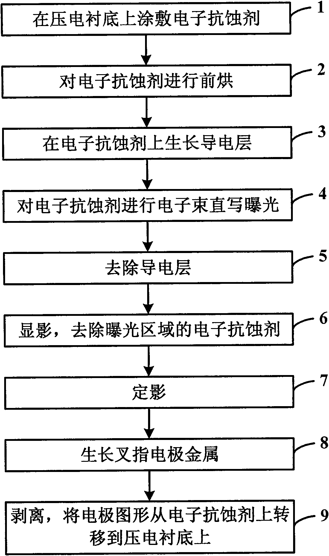
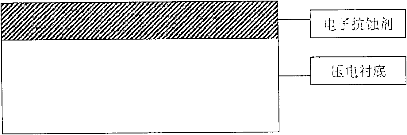
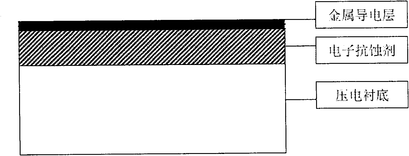
[0039] The invention adopts electron beam photolithography technology, which is an effective nano-processing method and has nano-level resolution. The invention mainly utilizes electron beam direct writing exposure to form the electronic resist concave vertical electrode pattern of the interdigital transducer whose spacing is less than 500nm on the piezoelectric substrate, and then the surface acoustic wave device can be produced by growing metal and stripping .

[0040] Such as figure 1 as shown, figure 1 It is a flow chart of a method for fabricating a surface acoustic wave device using electron beam direct writing exposure provided by the present invention, and the method specifically includes the following steps:

...


PUM

PropertyMeasurementUnit
Thicknessaaaaaaaaaa

Abstract

The invention discloses a method of producing surface acoustic wave devices by exposing X-rays in a direct writing way. Electron beam resist concave solid figures of an interdigital transducer are obtained by photoetching electron beams on a piezoelectric substrate, and various surface acoustic wave devices are produced with the stripping technology. The method of producing surface acoustic wave devices by exposing X-rays in a direct writing way comprises the following concrete steps: spreading the electron beam resist on the piezoelectric substrate; prebaking the electron beam resist; growingmetal material which has weak back scattering effect on the electron beam exposure; exposing the electron beams in a direct writing way; removing the metal layer; developing the electron beam resist;fixing the electron beam resist; growing interdigital electrode metal and stripping a beam resist masking film. An interdigital electrode produced with the method has steep and straight edges and good width control, and the method can be used for producing the surface acoustic wave devices which have the characteristic linewidth of less than 500nm. The method needs less process steps and is simple, stable and reliable.

Description

technical field [0001] The invention belongs to the technical field of micro-nano processing in microelectronics and surface acoustic wave devices, and particularly relates to a method for manufacturing surface acoustic wave devices using electron beam direct writing exposure, that is, a method for manufacturing electrodes with nanoscale interdigital transducers . Background technique [0002] According to the transmission properties of surface acoustic waves, for common piezoelectric media, when the working center frequency reaches 1 GHz, the interdigital electrodes will be smaller than 1 micron. With the operating frequency of mobile communication systems rising above 2GHz and the development of micro-sensing technology, surface acoustic wave devices are developing in the direction of high frequency and high performance, which poses challenges to the manufacture of surface acoustic wave devices and requires The width and spacing of the finger electrodes must be smaller an...

Claims


Application Information

Patent Timeline
IPC IPC(8): G03F7/00G03F7/20G03F7/039G03F7/42
Inventor 赵以贵刘明牛洁斌
Owner INST OF MICROELECTRONICS CHINESE ACAD OF SCI
Why Eureka
Try Eureka