

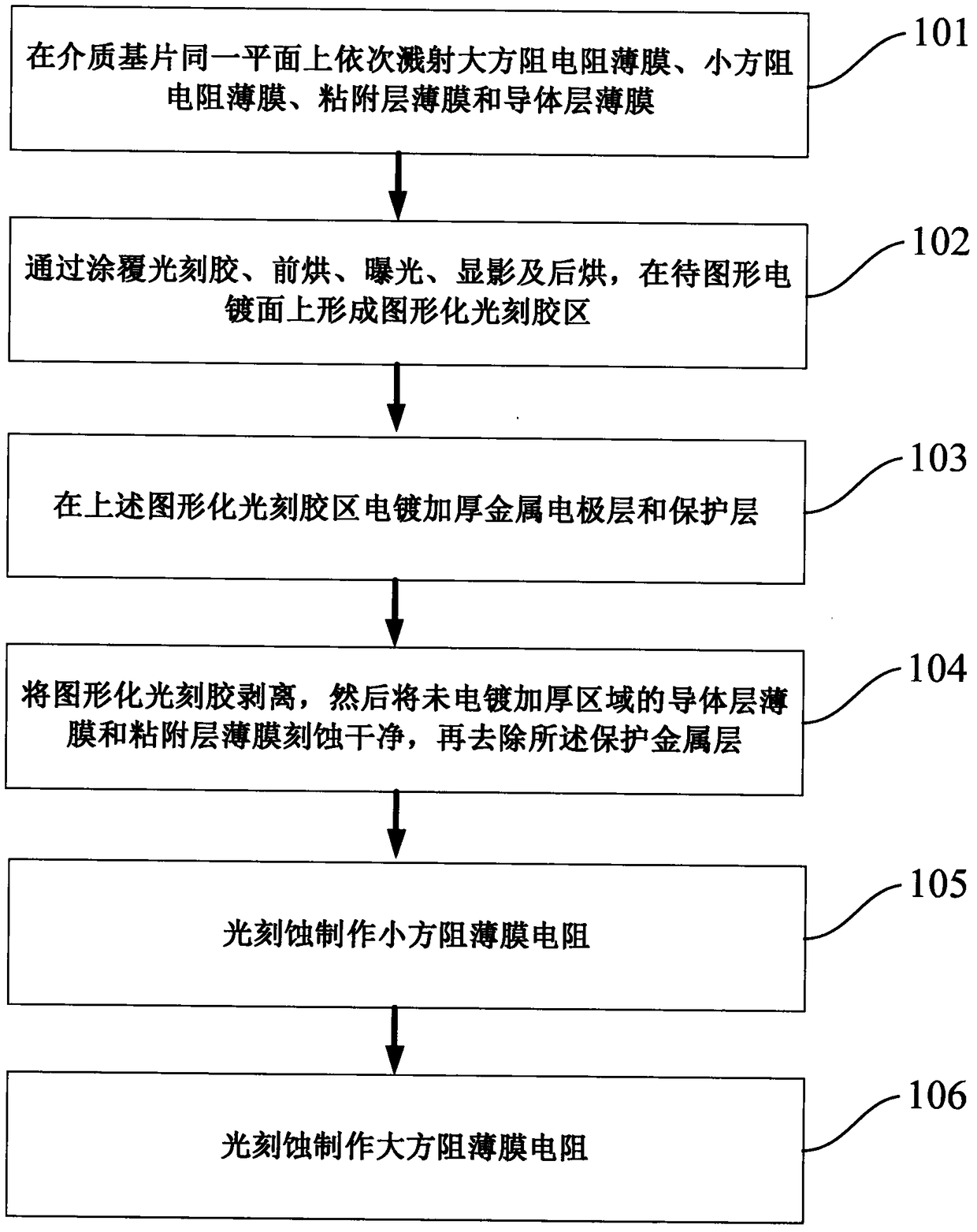
A Pattern Electroplating Method for Integrating Two Square Resistive Thin Film Circuits on the Same Plane of the Dielectric Substrate
A dielectric substrate and pattern electroplating technology, applied in circuits, electrical components, electrical solid devices, etc., can solve the problems of metal plating on the resistance layer and low pattern accuracy, reduce the risk of scratching the conductor pattern, and reduce the pattern resolution. High, improve the effect of circuit yield
- Summary
- Abstract
- Description
- Claims
- Application Information
AI Technical Summary
Problems solved by technology
Method used
Image

Examples
Embodiment 1
[0036] The NiCr / TaN / TiW / Au films are sequentially deposited on the same plane of the alumina dielectric substrate, taking the electroplating of thin film circuit patterns with two different square resistances of TaN and NiCr as an example:
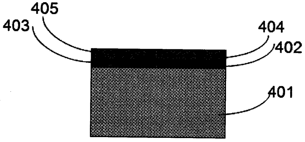
[0037] First, a dielectric substrate 401 is provided, such as Figure 3a As shown, the dielectric material is a 2in×2in square aluminum oxide substrate with a purity of 99.6%-100%, a thickness of 0.254mm, single-sided polishing, and a roughness of ≤1μin. After the dielectric substrate 401 is cleaned, NiCr / TaN / TiW / Au thin films are sequentially sputtered on the polished surface using a magnetron sputtering process. Among them, the large resistance film material 402 is a 200Ω / NiCr film, the small resistance film material 403 is a 9.5Ω / TaN film, the adhesive layer film material 404 is a TiW film, and the conductive layer film material 405 is an Au film.
[0038] Next, the electrode pattern is made into a photolithographic first mask. A laye...
Embodiment 2
[0044] NiCr / Ta / Ti / Au films are sequentially deposited on the same plane of the sapphire dielectric substrate, taking the electroplating of thin film circuit patterns with two different resistances of Ta and NiCr as an example:
[0045] First, a dielectric substrate 401 is provided, such as Figure 3a As shown, the dielectric material is a circular sapphire substrate with a diameter of 2in, a thickness of 0.254mm, double-sided polishing, and a roughness of ≤1μin. After the dielectric substrate 401 is cleaned, NiCr / Ta / Ti / Au thin films are sequentially sputtered on the polished surface using a magnetron sputtering process. Among them, the large resistance film material 402 is a 250Ω / NiCr film, the small resistance film material 403 is a 10Ω / Ta film, the adhesive layer film material 404 is a Ti film, and the conductor layer film material 405 is an Au film.
[0046] Next, the electrode pattern is made into a photolithographic first mask. Spin-coat a layer of RZJ-390PG photoresist...
PUM
 Abstract
Description
Claims
Application Information