Wafer grinding process

A grinding process and wafer technology, applied in the field of semiconductor wafer grinding process, can solve the problems of no adhesion, damage to bumps, easy to fall off, etc.

Inactive Publication Date: 2010-03-24
高宏明
View PDF0 Cites 10 Cited by
  • Summary
  • Abstract
  • Description
  • Claims
  • Application Information

AI Technical Summary

Problems solved by technology

However, the organic material layer is benzotriazoies or substituted benzotriazoles, known as Organic Solderability Preservatives (OSP). Attached to the work piece, when the thickness of the organic material layer of the organic solder protection film is too thick (about more than one micron), it is easy to fall off
However, in order to effectively protect the bumps, the thickness of the organic material layer should be tens of microns. There is no good adhesion between the organic material layer and the active surface of the wafer, and the protection for the bumps is limited.
In addition, when the abrasive tape is torn off, the adhesive force of the organic material layer to the wafer is smaller than the adhesive force between the abrasive tape and the organic material layer, which will cause the abrasive tape to be torn off together with the organic material, so that when the wafer is cut no further protection of the wafer
[0004] However, in another known technique, the method of protecting the bumps on the wafer during backgrinding is to use different from the general grinding tape, which has a base material and a special thickness of adhesive, the adhesive is a high thickness The film layer has strong adhesion, such as pressure-sensitive silica gel, acrylic adhesive (acrylicadhesive), and UV glue, to adhere to 10% to 60% of the bump area of ​​a wafer. Shape protection, when the crystal back is ground, the stress transmission between the grinding tape and the wafer still has to pass through these bumps, and the bonding interface between these bumps and the wafer will break
In addition, the bumps may be damaged when the grinding tape is removed, resulting in some bumps not being fixed on the active surface of the wafer

Method used


Image

  • Wafer grinding process
  • Wafer grinding process
  • Wafer grinding process

Examples


Embodiment Construction

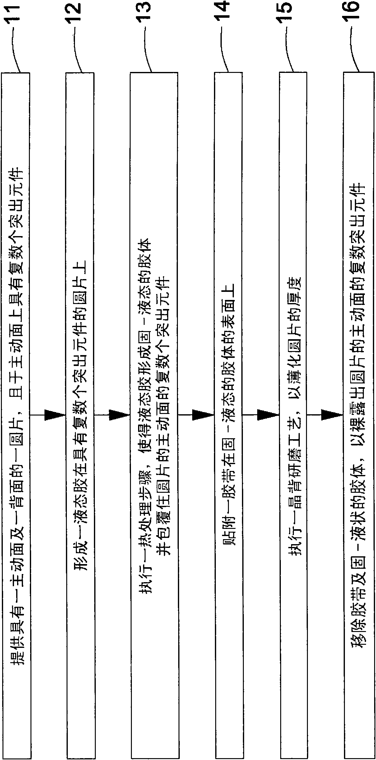
[0095] In order to have a further understanding of the purpose, structure, features, and functions of the present invention, the detailed description of the accompanying examples is as follows.

[0096] The direction discussed in the present invention is a crystal back grinding process of a semiconductor wafer. In order to provide a thorough understanding of the present invention, detailed implementation steps will be set forth in the following description. Here, the detailed steps of well-known grinding methods and other back-end processes are not described in detail to avoid unnecessary limitations of the present invention. However, for the preferred embodiments of the present invention, it will be described in detail as follows. However, in addition to these detailed descriptions, the present invention can also be widely implemented in other embodiments, and the scope of the present invention is not limited. The scope of the patent shall prevail.

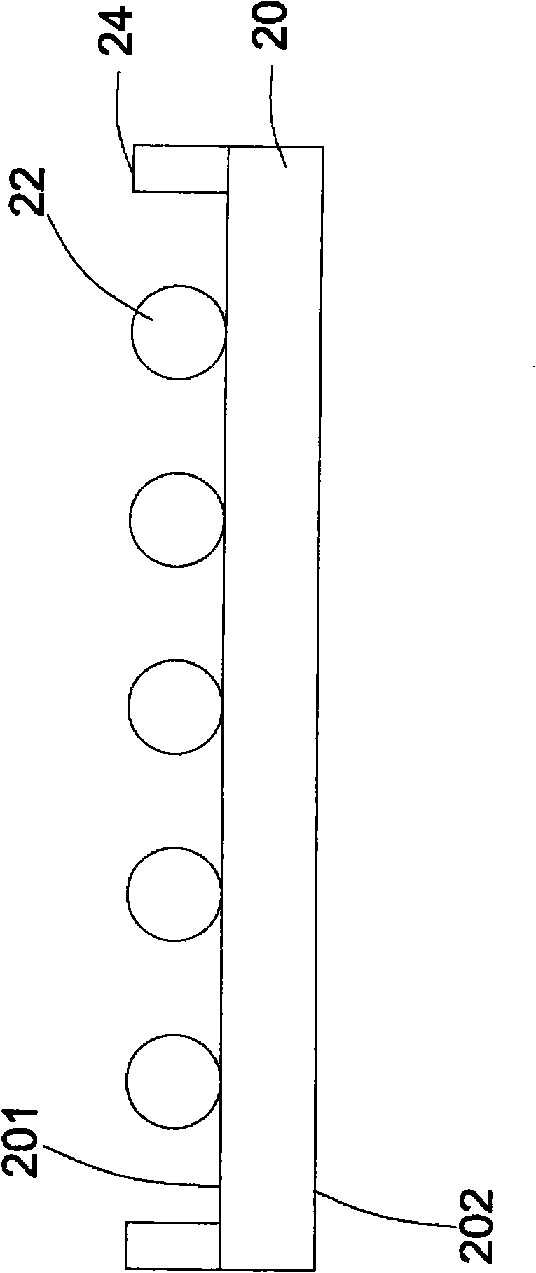
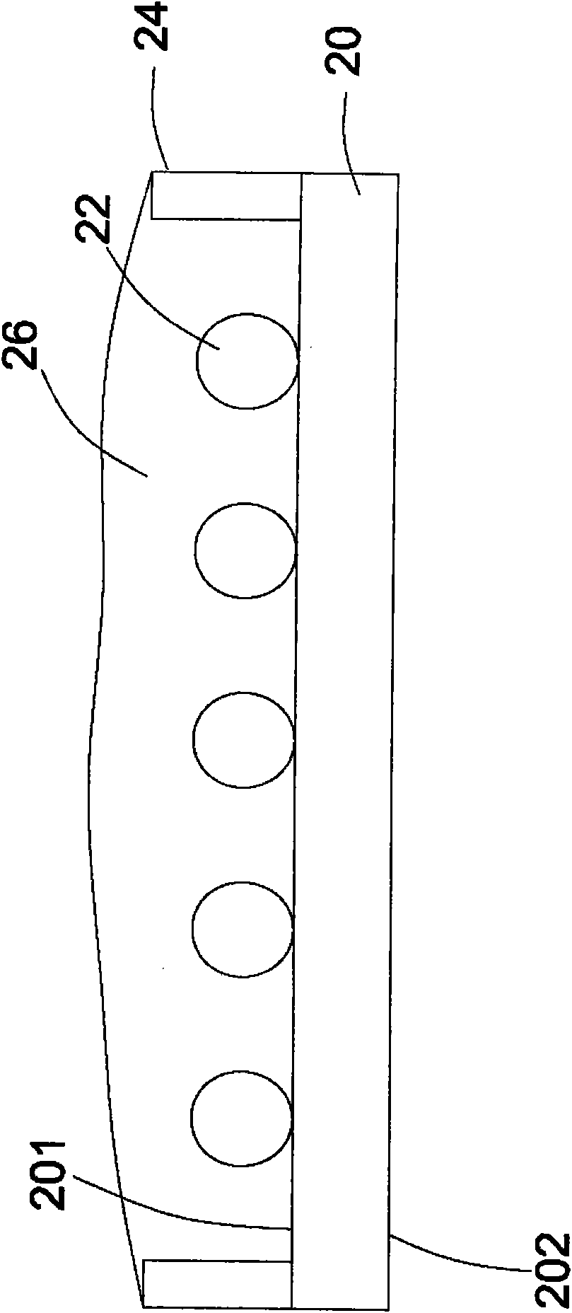
[0097] figure 1 It is ...


PUM


Abstract

The invention relates to a wafer grinding process which comprises the following steps: providing a wafer which comprises an active surface and a back surface, wherein, a plurality of protrudent components are formed on the active surface; forming a liquid adhesive for covering a plurality of protrudent components on the active surface of the wafer; pre-curing the liquid adhesive for forming a solid-liquid colloid for covering the active surface of the wafer and filling in a plurality of protrudent component; bonding an adhesive tape on the solid-liquid colloid; implementing the crystal back grinding process on the back surface of the wafer; and removing the adhesive tape and the solid-liquid colloid, thereby exposing a plurality of protrudent components on the active surface of the wafer.

Description

technical field [0001] The invention discloses a semiconductor wafer grinding process, and more particularly relates to the use of a protruding component that uses liquid glue to protect the active surface of the wafer during the crystal back grinding process. Background technique [0002] Wafer back grinding is a post-wafer process commonly used in semiconductors. Before the wafer is cut, a grinding tape is attached to the active surface of the wafer, and then the back of the wafer is ground and thinned, so that the cut chip has a Extremely thin thickness. However, the current wafer is often required to be provided with various additional protruding components, such as bumps, etc., on its active surface. During grinding tape on the active face of the wafer, these protruding components often fall off due to lack of protection. [0003] In order to properly protect the protruding components on the wafer during back grinding, a back grinding method for protruding packaged wa...

Claims


Application Information

Patent Timeline
Patent Type & Authority Applications(China)
IPC IPC(8): H01L21/00H01L21/304B24B37/04B24B29/02
Inventor 高宏明
Owner 高宏明
Why Eureka
Try Eureka