A kind of semiconductor device and its manufacturing method

A technology of semiconductors and manufacturing methods, applied in the field of semiconductor devices and their preparations, capable of solving the problems of dislocation of the first semiconductor chip and the second semiconductor chip, increased manufacturing costs, and low bonding stability, and achieving improved bonding stability , rich variety, anti-peeling effect

Active Publication Date: 2021-11-05
NANTONG HUIFENG ELECTRONICS TECH
View PDF5 Cites 0 Cited by
  • Summary
  • Abstract
  • Description
  • Claims
  • Application Information

AI Technical Summary

Problems solved by technology

However, in the actual packaging process, since the bonding stability of the first semiconductor chip and the second semiconductor chip is not high, it is easy to cause peeling dislocation between the first semiconductor chip and the second semiconductor chip in the process of encapsulating with resin, In turn, it affects the stability of the semiconductor stack package structure, which in turn leads to an increase in manufacturing costs

Method used


Image

  • A kind of semiconductor device and its manufacturing method
  • A kind of semiconductor device and its manufacturing method
  • A kind of semiconductor device and its manufacturing method

Examples


Embodiment Construction

[0032] In order to better understand the technical solutions of the present invention, the embodiments of the present invention will be described in detail below in conjunction with the accompanying drawings. Based on the embodiments of the present invention, all other embodiments obtained by persons of ordinary skill in the art without creative efforts fall within the protection scope of the present invention.

[0033] The present invention proposes a method for manufacturing a semiconductor device, comprising the following steps:

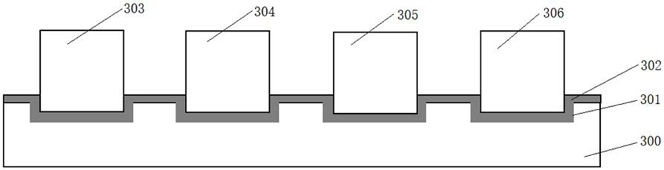
[0034] Step (1): providing a first carrier, setting a first elastic bonding layer on the first carrier, setting the first chip, the second chip, the third chip and the first chip on the first elastic bonding layer The fourth chip, the active surfaces of the first, second, third and fourth chips face the first elastic adhesive layer, and a part of each of the first, second, third and fourth chips is embedded in the first elastic adhesive layer.

...


PUM


Abstract

The present invention relates to a semiconductor device and a manufacturing method thereof, by forming first and second grooves in the first, second, third and fourth chips respectively , third, and fourth blind holes, and respectively form first, second, third, and fourth protrusions on the respective back surfaces of the fifth, sixth, seventh, and eighth chips, and The side surfaces of the second, third, and fourth protrusions respectively form through holes, and then in the subsequent bonding process, in the first, second, third, and fourth grooves and the first, second, and third 1. Adhesive material is set in the fourth blind hole, and the fifth, sixth, seventh, and eighth chips are correspondingly set in the first, second, third, and fourth grooves, so that the first, the first Two, third, and fourth protrusions are respectively embedded in the corresponding first, second, third, and fourth blind holes, and a part of the bonding material in each blind hole is embedded in each through hole of each protrusion .

Description

technical field [0001] The invention relates to the field of semiconductor packaging, in particular to a semiconductor device and a preparation method thereof. Background technique [0002] In the existing semiconductor stack packaging technology, usually an adhesive material is directly provided between the first semiconductor chip and the second semiconductor chip to complete the bonding of the first semiconductor chip and the second semiconductor chip, and then use the resin material to package the above-mentioned bonding the completed first semiconductor chip and the second semiconductor chip. However, in the actual packaging process, since the bonding stability of the first semiconductor chip and the second semiconductor chip is not high, it is easy to cause peeling dislocation between the first semiconductor chip and the second semiconductor chip in the process of encapsulating with resin, This further affects the stability of the semiconductor stack package structure...

Claims


Application Information

Patent Timeline
Patent Type & Authority Patents(China)
IPC IPC(8): H01L21/50H01L21/56H01L23/31
CPCH01L21/50H01L21/561H01L21/568H01L23/3107
Inventor 宋小波石明华蔡成俊陈健
Owner NANTONG HUIFENG ELECTRONICS TECH
Why Eureka
Try Eureka