Electronic package and manufacturing method thereof
An electronic packaging and plastic packaging technology, which is applied in the direction of circuits, electrical components, and electrical solid devices, can solve the problem of unsatisfactory signal performance size and testability, unsatisfactory electrical performance and size, and complex manufacturing And other issues
- Summary
- Abstract
- Description
- Claims
- Application Information
AI Technical Summary
Problems solved by technology
Method used
Image

Examples
Embodiment Construction
[0029] Detailed Description of Preferred Embodiments
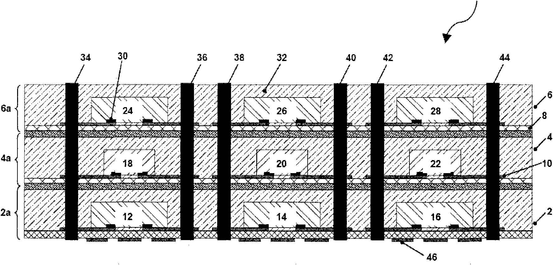
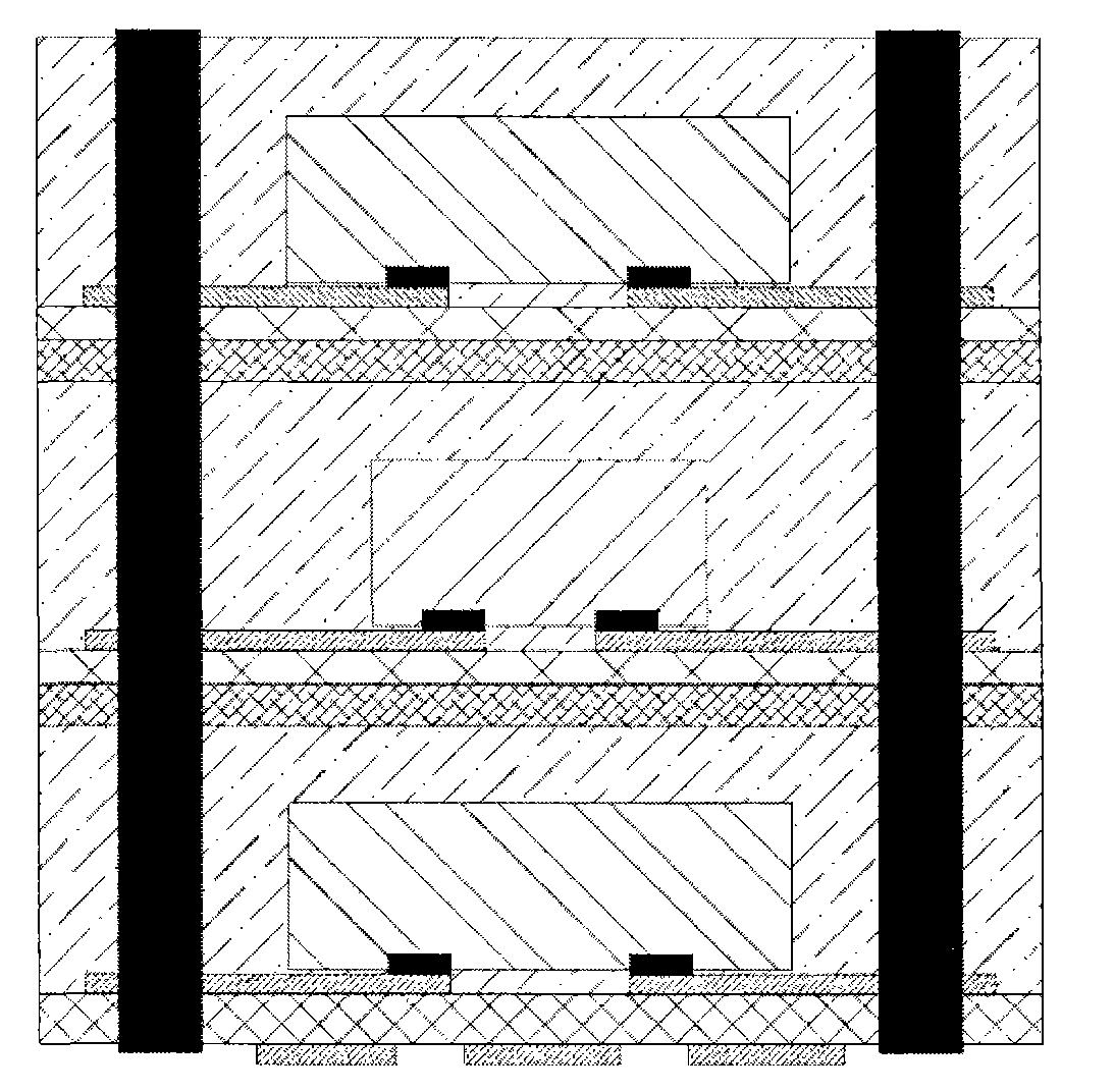
[0030] The prior art has disclosed many different types of electronic packaging systems. For example, US Pat. No. 5,128,831 discloses a module package in which spacers are stacked alternately. US Patent 7,279,786 discloses a package-on-package system in which the upper substrate has a recess on its bottom surface for receiving one or more semiconductor chips. US Patent 7,317,256 discloses an electronic device package comprising wafers, each wafer having through-silicon vias, and two packaging layers connected by solder joints. US Patent Document 2007 / 0216004 discloses a semiconductor device with chips embedded in plastic material. US Patent Document 2008 / 0169546 discloses a semiconductor chip package stack with one wafer mold package stacked on top of the other. The present invention proposes a different electronic package that has at least some advantages over existing devices. For clarity of description, please note ...
PUM
 Abstract
Description
Claims
Application Information
 - R&D Engineer
- R&D Manager
- IP Professional
- Industry Leading Data Capabilities
- Powerful AI technology
- Patent DNA Extraction
Browse by: Latest US Patents, China's latest patents, Technical Efficacy Thesaurus, Application Domain, Technology Topic.
© 2024 PatSnap. All rights reserved.Legal|Privacy policy|Modern Slavery Act Transparency Statement|Sitemap