Printing circuit board

A printed circuit board and electrical connection technology, which is applied to printed circuits, printed circuits, printed circuit components, etc., can solve problems such as the influence of analog components on work, and achieve the effect of improving work quality

Inactive Publication Date: 2010-03-31
SHENZHEN FUTAIHONG PRECISION IND CO LTD +1
View PDF0 Cites 1 Cited by
  • Summary
  • Abstract
  • Description
  • Claims
  • Application Information

AI Technical Summary

Problems solved by technology

However, the electromagnetic interference signal in the external environment will be coupled to the analog components through the shielding cover. Since the area of ​​the analog formation is very small compared with the digital formation, the external electromagnetic interference signal cannot be absorbed by the analog formation immediately, and can only be shielded all the time. Continuous vibration in the cover will still have a great impact on the work of analog components

Method used


Image

  • Printing circuit board

Examples


Embodiment Construction

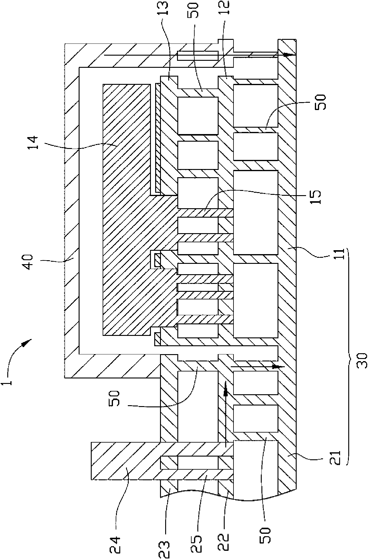
[0008] The present invention will be further described in detail below in conjunction with the accompanying drawings.

[0009] see figure 1 , is a printed circuit board 1 provided by an embodiment of the present invention, which includes an analog area 10 , a digital area 20 and a shield 40 .

[0010] The simulation area 10 includes a simulation ground layer 11 , a simulation wiring layer 12 , a simulation bearing layer 13 and a simulation component 14 . The simulated wiring layer 12 and the simulated bearing layer 13 are sequentially stacked on the simulated ground layer 11, and the simulated wiring layer 12 is electrically connected to the simulated ground layer 11 through a conductive material 50, and the simulated bearing layer 12 is connected to the simulated ground layer 11. The above-mentioned analog wiring layers 12 are electrically connected through a conductive material 50 . The analog component 14 includes a plurality of analog ground pins 15 , the analog componen...


PUM


Abstract

The invention relates to a printing circuit board, which comprises an analog area and a digital area, wherein the analog area comprises an analog formation, an analog wiring layer and an analog bearing layer, wherein the analog wiring layer and the analog bearing layer are electrically stacked on the analog formation sequentially and an analog element which is adhered to the analog bearing layer and electrically connected with the analog wiring layer through analog grounding pins; the digital area comprises a digital formation, a digital wiring layer and a digital bearing layer, wherein the digital wiring layer and the digital bearing layer are electrically stacked on the digital formation sequentially and a digital element which is adhered to the digital bearing layer and electrically connected with the digital wiring layer through digital grounding pins; the analog formation is connected with the digital formation to form a main formation with a larger area; the analog wiring layer and the digital wiring layer are separated mutually; and the analog bearing layer and the digital bearing layer are separated mutually. The printing circuit board can make an electromagnetic interference signal absorbed quickly by the main formation with the larger area and prevent the electromagnetic interference signal generated by the digital element from transmitting to the analog element.

Description

technical field [0001] The invention relates to a printed circuit board. Background technique [0002] Printed circuit boards are generally formed by stacking multiple layers in sequence. Taking a printed circuit board with only three layers as an example, the printed circuit board includes a bearing layer, a wiring layer and a ground layer. The carrying layer and the wiring layer are sequentially and electrically stacked on the ground layer. The carrying layer is used to carry various electronic components, the wiring layer is used to electrically connect the pins of each electronic component, and the ground layer is used as a reference point of zero potential of each circuit. Analog components and digital components are usually arranged on the printed circuit board, and a shielding cover electrically connected to the ground is usually covered on the analog components to prevent external electromagnetic waves from interfering with the analog components. Since the digital...

Claims


Application Information

Patent Timeline
Patent Type & Authority Applications(China)
IPC IPC(8): H05K3/46H05K9/00
CPCH05K2201/09972H05K1/0216H05K1/0243H05K2201/09318H05K2201/10083H05K2201/10371
Inventor 李明峰
Owner SHENZHEN FUTAIHONG PRECISION IND CO LTD
Why Eureka
Try Eureka