
Surface structure of silicon crystal cell and manufacturing method thereof

A technology of battery surface and manufacturing method, applied in the direction of final product manufacturing, sustainable manufacturing/processing, circuit, etc., can solve the problems of low photoelectric conversion efficiency, fragmentation, thin thickness of crystalline battery, etc., to improve photoelectric conversion efficiency, An effect that reduces the chance of fragmentation

Inactive Publication Date: 2010-05-12
MOTECH INDUSTRIES
View PDF1 Cites 10 Cited by
  • Summary
  • Abstract
  • Description
  • Claims
  • Application Information

AI Technical Summary

Problems solved by technology

In the prior art, most of the surfaces of solar silicon crystal cells are simply acid-etched or alkali-etched. Most of the solar silicon crystal cells produced by these two etching methods have a large roughness coefficient in most of the surface structures. Moreover, the thickness of the crystal battery is relatively thin, which is easy to cause fragments in the production process
In addition, the photoelectric conversion efficiency of the cells manufactured by the above two methods is not high

Method used


Image

  • Surface structure of silicon crystal cell and manufacturing method thereof
  • Surface structure of silicon crystal cell and manufacturing method thereof
  • Surface structure of silicon crystal cell and manufacturing method thereof

Examples


Embodiment Construction

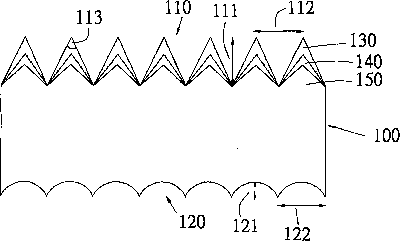
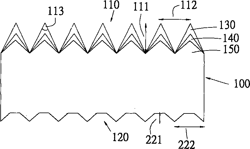
[0021] figure 1 with figure 2 It is a schematic diagram of two embodiments of the surface structure of the silicon crystal battery proposed by the present invention. Such as figure 1 As shown, the surface structure of the silicon crystal battery includes: a main body 100 , the main body 100 has a front surface 110 and a back surface 120 , and the roughness coefficient of the structure of the front surface 110 is greater than that of the structure of the back surface 120 . The surface morphology of the microstructure of the front surface 110 includes a plurality of cones, and the direction of the apex of the cones is away from the main body 100 . In addition, the surface morphology of the microstructure of the back surface 120 includes a plurality of arcs. figure 2 Showing another implementation structure, the surface morphology of the microstructure on the back surface 120 includes a plurality of polygonal structures.

[0022] figure 1 wherein, the height 111 of the fro...


PUM

PropertyMeasurementUnit
Heightaaaaaaaaaa
Vertex angleaaaaaaaaaa
Depthaaaaaaaaaa

Abstract

The invention discloses a surface structure of a silicon crystal cell and a manufacturing method thereof. The surface structure of the silicon crystal cell comprises a main body, the main body is provided with a front surface and a back surface, wherein the roughness coefficient of the front surface of the main body is larger than that of the back surface of the main body; the surface morphology of a front surface microstructure comprises a plurality of tapering bodies; and the surface morphology of a back surface microstructure comprises a plurality of arc bodies or polygonal bodies. The invention enables the back surface of the surface structure of the silicon crystal cell to be flatter than the front surface of the same, thereby enhancing the photoelectric conversion efficiency and reducing the fragmenting probability in the manufacture process.

Description

technical field [0001] The invention relates to a silicon crystal battery, in particular to a surface structure of a silicon crystal battery and a manufacturing method thereof. Background technique [0002] At present, with the rising awareness of environmental protection and the prevailing mainstream value of pursuing energy saving and carbon reduction, the trend of green energy replacing petroleum energy is becoming more and more obvious. Therefore, related industries such as solar energy are developing vigorously to meet the needs of the market, especially the demand for solar cells increase is more pronounced. [0003] The photoelectric conversion efficiency of solar silicon cells is one of the most important parameters for evaluating the pros and cons. In the prior art, most of the surfaces of solar silicon crystal cells are simply acid-etched or alkali-etched. Most of the solar silicon crystal cells produced by these two etching methods have a large roughness coeffici...

Claims


Application Information

Patent Timeline
IPC IPC(8): H01L31/052H01L31/0236H01L31/18H01L31/068
CPCY02E10/50Y02E10/547Y02P70/50
Inventor 林勉良林景颖杜庆豪
Owner MOTECH INDUSTRIES
Learn More