Non-volatile storage with individually controllable shield plates between storage elements

A non-volatile storage and shielding plate technology, applied in electrical components, information storage, read-only memory, etc., can solve the problem of reducing the coupling rate from the control gate to the floating gate, reducing the size of the device, and expanding the threshold voltage distribution And other issues

Active Publication Date: 2010-05-19
SANDISK TECH LLC
View PDF11 Cites 5 Cited by
  • Summary
  • Abstract
  • Description
  • Claims
  • Application Information

AI Technical Summary

Problems solved by technology

[0008] However, as device dimensions shrink, various challenges arise
For example, floating gate-to-floating gate coupling become

Method used


Image

  • Non-volatile storage with individually controllable shield plates between storage elements
  • Non-volatile storage with individually controllable shield plates between storage elements
  • Non-volatile storage with individually controllable shield plates between storage elements

Examples


Embodiment Construction

[0052] The present invention provides a non-volatile memory device with individually controllable shielding plates between memory elements.

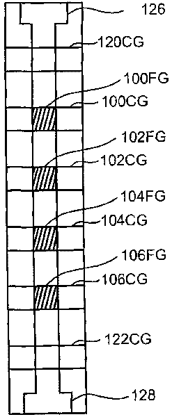
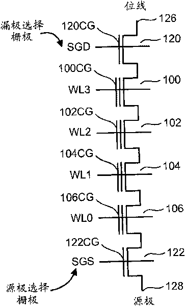
[0053] One example of a memory system suitable for implementing the present invention uses a NAND flash memory structure that includes multiple transistors arranged in series between two select gates. Transistors and select gates connected in series are called NAND strings. figure 1 is a top view showing one NAND string. figure 2 is its equivalent circuit. figure 1 with figure 2 The depicted NAND string includes four transistors 100 , 102 , 104 and 106 in series and sandwiched between a first select gate 120 and a second select gate 122 . Select gate 120 gates the NAND string connection to bit line 126 . Select gate 122 gates the NAND string connection to source line 128 . Select gate 120 is controlled by applying an appropriate voltage to control gate 120CG. Select gate 122 is controlled by applying an appropriate voltage to con...


PUM


Abstract

A non-volatile storage having individually controllable shield plates between storage elements. The shield plates are formed by depositing a conductive material such as doped polysilicon between storage elements and their associated word lines, and providing contacts for the shield plates. The shield plates reduce electromagnetic coupling between floating gates of the storage elements, and can beused to optimize programming, read and erase operations. In one approach, the shield plates provide a field induced conductivity between storage elements in a NAND string during a sense operation so that source/drain implants are not needed in the substrate. In some control schemes, alternating high and low voltages are applied to the shield plates. In other control schemes, a common voltage is applied to the shield plates.

Description

technical field [0001] The present invention relates to non-volatile memory. Background technique [0002] Semiconductor memories have become increasingly common in various electronic devices. For example, non-volatile semiconductor memory is used in cellular telephones, digital cameras, personal digital assistants, mobile computing devices, non-mobile computing devices, and other devices. Electrically Erasable Programmable Read-Only Memory (EEPROM) and flash memory are among the most popular non-volatile semiconductor memories. With flash memory—which is also a type of EEPROM—the contents of the entire memory array or a portion of the memory can be erased in one step compared to conventional full-featured EEPROMs. [0003] Both conventional EEPROM and flash memory use a floating gate that is positioned over and insulated from a channel region in a semiconductor substrate. The floating gate is located between the source and drain regions. The control gate is provided ove...

Claims


Application Information

Patent Timeline
IPC IPC(8): G11C16/00H01L27/115
CPCH01L27/11524G11C16/10H01L27/11521G11C16/0483H01L27/115H01L27/0207H01L27/11519H10B41/10H10B41/35H10B69/00H10B41/30
Inventor 东谷政昭
Owner SANDISK TECH LLC
Why Eureka
Try Eureka