


Quick Research
Generate reliable direction feasibility study reports for your R&D in just a few steps.

Technical Q&A
Discover and master advanced knowledge NOW. Basics, ideas, possibilities, all at once.

Find Solutions
As an expert in R&D theories, this can generate solutions to your technical problems instantly.

Evaluate Feasibility
Analyze your overall solution with one click, know your potential R&D risks in advance.

Monitor Landscape
Get weekly tech updates, stay abreast of the latest tech innovations and key insights.
Ceramic substrate for three-dimensional packaging of multi-chip system and packaging method thereof
A technology of ceramic substrate and three-dimensional packaging, applied in the field of ceramic substrate
- Summary
- Abstract
- Description
- Claims
- Application Information
AI Technical Summary
Problems solved by technology
Method used
Image

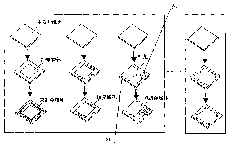
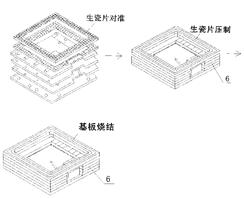
Examples
Embodiment Construction
[0040] In order to further understand the purpose of the present invention, the packaging structure and its features, the detailed description is as follows in conjunction with the accompanying drawings:
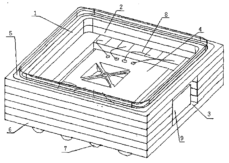
[0041] A ceramic substrate for three-dimensional packaging of a multi-chip system according to the present invention includes a laminated ceramic 6, a first cavity 2 is formed in the horizontal plane of the laminated ceramic 6 to accommodate the first chip, and the first cavity A cover plate 1 is arranged above the body 2, and the cover plate 1 seals the first cavity 2 and the first chip 4. It is characterized in that: the side wall of the laminated ceramic 6 has a The second cavity 3 of a cavity 2 is to accommodate the second chip 9, and a pad interconnected with the second chip is arranged in the second cavity 3, and the pad is electrically connected to the first cavity. interconnection. The cover plate seals the first cavity 2 and the first chip 4 through a sealing membe...
PUM
 Abstract
Description
Claims
Application Information
 - R&D Engineer
- R&D Manager
- IP Professional
- Industry Leading Data Capabilities
- Powerful AI technology
- Patent DNA Extraction
Browse by: Latest US Patents, China's latest patents, Technical Efficacy Thesaurus, Application Domain, Technology Topic, Popular Technical Reports.
© 2024 PatSnap. All rights reserved.Legal|Privacy policy|Modern Slavery Act Transparency Statement|Sitemap|About US| Contact US: help@patsnap.com