Method for controlling semiconductor photosensitive component

A technology of photosensitive device and control method, which is applied to electrical components, parts of color TV, parts of TV system, etc., to achieve the effect of simple control method and high image resolution

Active Publication Date: 2010-05-26
SUZHOU ORIENTAL SEMICONDUCTOR CO LTD
View PDF0 Cites 8 Cited by
  • Summary
  • Abstract
  • Description
  • Claims
  • Application Information

AI Technical Summary

Problems solved by technology

[0009] The technical problem to be solved by the present invention is to reduce the circuit complexity of a single pixel unit in a CMOS image sensor and improve the pixel density of the image sensor.

Method used


Image

  • Method for controlling semiconductor photosensitive component
  • Method for controlling semiconductor photosensitive component
  • Method for controlling semiconductor photosensitive component

Examples


Embodiment Construction

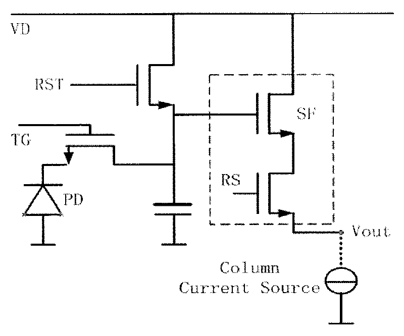
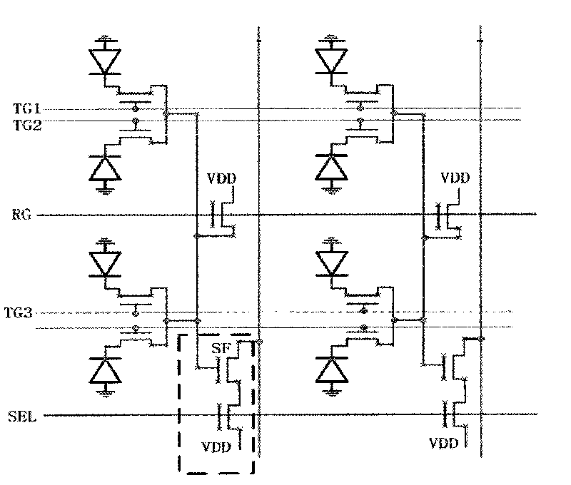
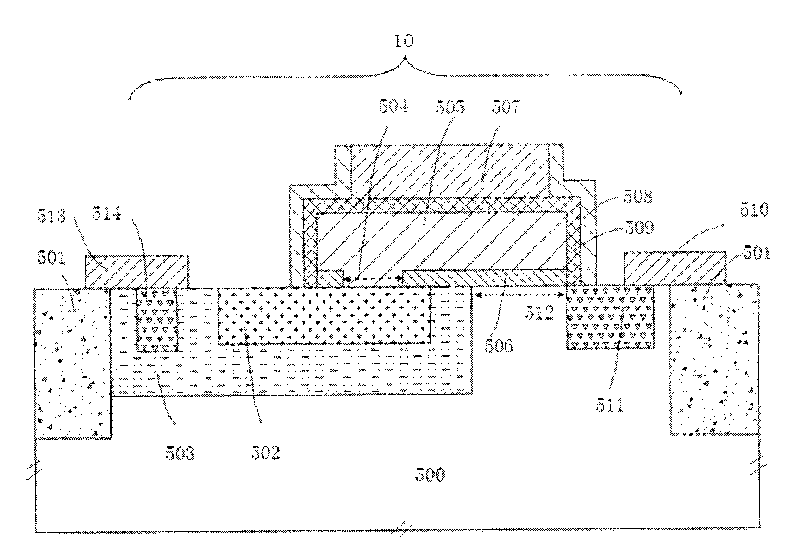
[0038] Hereinafter, three exemplary embodiments of the present invention will be described in detail with reference to the accompanying drawings. In the drawings, the thicknesses of layers and regions are exaggerated for convenience of illustration, and the shown sizes do not represent actual sizes. The referenced figures are schematic illustrations of idealized embodiments of the invention, and the illustrated embodiments of the invention should not be construed as limited to the particular shapes of regions illustrated in the figures but are to include resulting shapes, such as manufacturing-induced deviations. For example, the curves obtained by etching are usually curved or rounded, but in the embodiment of the present invention, they are all represented by rectangles. The representation in the figure is schematic, but this should not be considered as limiting the scope of the present invention. Also in the following description, the terms wafer and substrate used may be u...


PUM


Abstract

The invention discloses a semiconductor photosensitive component comprising a source electrode, a drain electrode, a control grid electrode, a floating grid region, an underlay and a p-n junction diode used for connecting the floating grid region and the drain electrode, wherein the floating grid region of the semiconductor component is used for storing electric charges. The floating grid potential of the semiconductor component is relevant to radiation intensity and time of light, so that the semiconductor component can serve as the semiconductor photosensitive component. An array can be formed by the semiconductor photosensitive component, thereby forming am image sensor. The invention discloses a method for controlling the semiconductor photosensitive component, comprising the following steps of: resetting, light sensation and reading. The semiconductor photosensitive component can simplify the design of single pixel unit in the traditional image sensor and reduce the area occupied by the single pixel unit, thereby increasing the pixel density of an image sensing chip, increasing the resolution of the image sensing chip and reducing the manufacture cost; moreover, the control method and a control circuit are simpler.

Description

technical field [0001] The invention relates to a semiconductor photosensitive device and an array, in particular to a structure and a manufacturing method of the semiconductor photosensitive device and the array. The invention also relates to the operating principle of a semiconductor photosensitive device and array. Background technique [0002] Image sensors are semiconductor devices used to convert optical signals into electrical signals. Image sensor chips (Image Sensors) composed of image sensor devices are widely used in multimedia products such as digital cameras, video cameras, and mobile phones. [0003] Currently, there are mainly two types of image sensors: a charge coupled device (Charge Coupled Device, CCD) image sensor and a CMOS (Complementary Metal-Oxide-Semiconductor) image sensor. Charge-coupled devices have the advantages of high image quality and low noise, but their production costs are also high, and they are not suitable for integration with peripher...

Claims


Application Information

Patent Timeline
Patent Type & Authority Applications(China)
IPC IPC(8): H04N3/15H04N5/335
Inventor 王鹏飞刘磊刘伟张卫
Owner SUZHOU ORIENTAL SEMICONDUCTOR CO LTD
Why Eureka
Try Eureka