Ceramic chip assembly and manufacturing method thereof

A chip and ceramic technology, applied in the field of ceramic chip components, can solve the problems of reduced adhesive strength, difficulty in providing ceramic chip components, and difficulty in protecting ceramic chips

Inactive Publication Date: 2011-08-31
JOINSET
View PDF0 Cites 0 Cited by
  • Summary
  • Abstract
  • Description
  • Claims
  • Application Information

AI Technical Summary

Problems solved by technology

In addition, the lead frame will be easily cut in the thin thickness direction
[0018] In addition, since the hot melt adhesive is melted by heat, the adhesive strength decreases significantly at high temperature, making it difficult to protect the ceramic chip
[0019] Also, the ceramic chip applied to the lead frame is a ceramic bare chip having a thin single layer and not including internal electrodes formed therein, so that it is difficult to provide a ceramic chip assembly having various properties

Method used


Image

  • Ceramic chip assembly and manufacturing method thereof
  • Ceramic chip assembly and manufacturing method thereof
  • Ceramic chip assembly and manufacturing method thereof

Examples


Embodiment Construction

[0055] Now, preferred embodiments of the present invention will be described in detail with reference to the accompanying drawings.

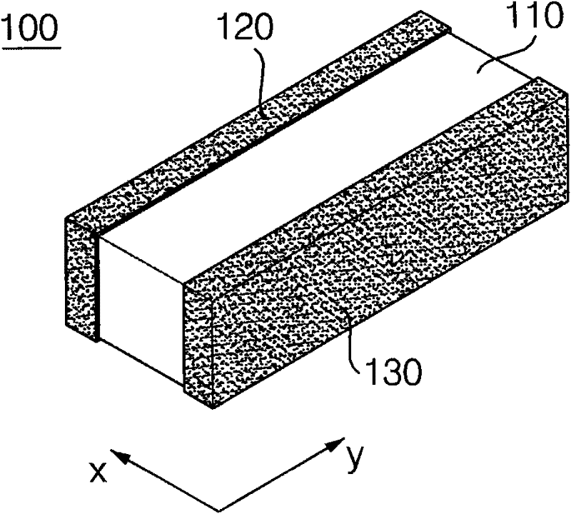
[0056] figure 2 is a view showing an exemplary ceramic chip 100 applied to a ceramic chip assembly according to an embodiment.

[0057] refer to figure 2 , the ceramic chip 100 includes a ceramic base 110 and external electrodes 120 , 130 .

[0058] The ceramic base 110 has a hexahedral shape and electrical properties. External electrodes 120 and 130 are oppositely formed on both side surfaces of the ceramic base 110 .

[0059] According to an embodiment, the length, thickness, and width of the ceramic chip 100 may be about 1 mm, about 0.30 mm, and about 0.5 mm, respectively, but are not limited thereto.

[0060] If the size of the ceramic chip 100 is too small, automation of tape and reel may encounter difficulty when manufacturing a ceramic chip assembly.

[0061] The external electrodes 120 and 130 may be formed at both ends of the cer...


PUM

PropertyMeasurementUnit
thicknessaaaaaaaaaa
thicknessaaaaaaaaaa
diameteraaaaaaaaaa

Abstract

A ceramic chip assembly is provided. The ceramic chip assembly includes a ceramic base, a plurality of external electrodes, a pair of cylindrical metal lead wires, and an insulating protection material. The ceramic base has electrical characteristics of a semiconductor. The pair of external electrodes is oppositely formed on both side surfaces of the ceramic base, respectively. The cylindrical metal lead wire has one end thereof electrically and mechanically connected to the external electrodes by an electrical conductive adhesive, respectively, and has an external diameter identical to or greater than the thickness of the ceramic base. The insulating protection material includes a pair of insulating films and an insulating coating layer.

Description

technical field [0001] The present invention relates to a ceramic chip module, and more particularly, to a ceramic chip module having a thin thickness and improved mechanical strength, the ceramic chip module including an insulating protective layer having a uniform thickness. In addition, the present invention relates to a ceramic chip assembly whose internal ceramic chips are protected from external loads, shocks, and friction, and are hardly affected by external environments. In addition, the present invention relates to a ceramic chip assembly having high productivity and high economic efficiency due to its low material cost and continuous operation in a reel tape manner. Background technique [0002] As a method of mounting a ceramic chip having electrical properties of a semiconductor (such as a thermistor, a magnetic substance, and a piezoelectric body) on a printed circuit board (PCB), there is a method in which a metal lead or lead After the frame is soldered to th...

Claims


Application Information

Patent Timeline
Patent Type & Authority Patents(China)
IPC IPC(8): H01G4/00H01G4/12H01L41/08H01L41/24H01F1/10H01F1/34H01C7/04
CPCH01L2924/0002H01L2924/00H01G4/12H01L23/48H05K13/04H01L23/02
Inventor 金善基李硕珠
Owner JOINSET
Why Eureka
Try Eureka