Wide visual angle LCD array substrate and manufacturing method thereof

A technology for liquid crystal displays and array substrates, used in semiconductor/solid-state device manufacturing, instruments, electrical solid-state devices, etc. Application foreground, the effect of expanding the viewing angle

Inactive Publication Date: 2010-06-09
BOE TECH GRP CO LTD
View PDF0 Cites 6 Cited by
  • Summary
  • Abstract
  • Description
  • Claims
  • Application Information

AI Technical Summary

Problems solved by technology

The TN+film mode has very limited improvement on the viewing angle. The viewing angle improvement is limited to the range of 140° horizontally and 100° vertically. It is generally only used in notebook computers and desktop monitors, and is not suitable for large-size LCD TV applications; MVA mode requires A complex raised structure is manufactured on the side of the color filter substrate (color filter), which increases the manufacturing cost; the PVA mode requires the pixel electrode to be made into a complex slit structure, which affects the light utilization efficiency; while the IPS mode and the FFS mode High process control precision is required, the manufacturing process is difficult, and the contrast is affected

Method used


Image

  • Wide visual angle LCD array substrate and manufacturing method thereof
  • Wide visual angle LCD array substrate and manufacturing method thereof
  • Wide visual angle LCD array substrate and manufacturing method thereof

Examples


Embodiment Construction

[0045] The technical solutions of the present invention will be described in further detail below with reference to the accompanying drawings and embodiments.

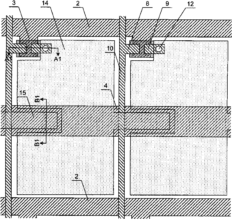
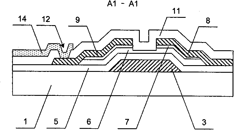
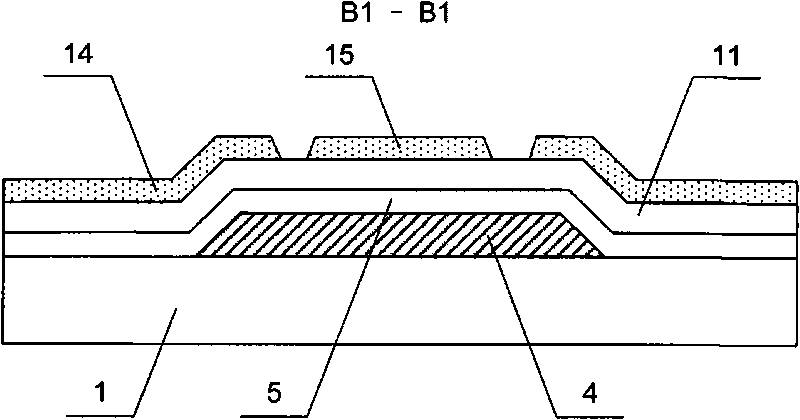
[0046] figure 1 It is a schematic structural view of the array substrate of the wide viewing angle liquid crystal display of the present invention, figure 2 for figure 1 The sectional view of A1-A1 direction in the middle, image 3 for figure 1 The cross-sectional view of B1-B1 in the middle. Such as Figure 1 ~ Figure 3As shown, the main structure of the wide viewing angle LCD array substrate of the present invention includes gate lines 2, data lines 10 and thin film transistors (Thin Film Transistor, TFT for short) formed on the substrate; several gate lines 2 and several data lines 10 Several pixel areas are defined, and a thin film transistor is formed in each pixel area, and is located at the intersection of the gate line 2 and the data line 10; each pixel area is also formed with a pixel electrode 14 and at...


PUM

PropertyMeasurementUnit
widthaaaaaaaaaa

Abstract

The invention relates to a wide visual angle LCD array substrate and a manufacturing method thereof. The array substrate comprises a grid line and a data line formed on the substrate, wherein a thin film transistor and a pixel electrode are formed in a pixel region limited by the grid line and the data line; at least one extension electrode is formed in the pixel region; and a slit used for generating a transverse electric field is formed between the at least one extension electrode and the pixel electrode. The manufacturing method comprises the following steps of: forming a pattern comprising the grid line, a grid electrode, the data line, a source electrode, a leakage electrode, a TFT channel region and a passivation layer on the substrate; depositing a transparent conductive thin film; forming the pattern comprising the pixel electrode and the at least one extension electrode in the pixel region by composition process; and forming the slit used for generating the transverse electric field between the at least one extension electrode and the pixel electrode. The array substrate expands visual angles in surrounding multiple directions, achieves the purpose that the visual angles at various angles are uniform, and simplifies the structure and manufacturing process of the array substrate at the same time.

Description

technical field [0001] The invention relates to a liquid crystal display and a manufacturing method thereof, in particular to a wide viewing angle liquid crystal display array substrate and a manufacturing method thereof. Background technique [0002] The market of liquid crystal display is growing rapidly, and the application fields are continuously expanding, especially the application of large-size liquid crystal TV, which requires the liquid crystal display to have a wide range of viewing angles. The liquid crystal display includes an array substrate and a color filter substrate in a cell, and a liquid crystal is arranged between them. The liquid crystal is deflected under the action of voltage, and the degree of deflection of the liquid crystal can be controlled by controlling the magnitude of the voltage, so as to achieve the purpose of modulating the transmittance (display gray scale). [0003] Due to the optical anisotropy of liquid crystals, liquid crystal displays...

Claims


Application Information

Patent Timeline
Patent Type & Authority Applications(China)
IPC IPC(8): G02F1/1362G02F1/1343H01L21/84H01L27/12
CPCH01L27/124
Inventor 张俊瑞邵喜斌尹海军
Owner BOE TECH GRP CO LTD
Why Eureka
Try Eureka