
Surface artificial electromagnetic material applied to directional radiation modulation

An artificial electromagnetic material and directional radiation technology, applied in the direction of circuits, magnetic objects, electrical components, etc., can solve the problems of physical phenomena that do not support the surface plasmon mode, and achieve the effect of high refractive index, simple structure processing, and low cost

Inactive Publication Date: 2010-06-09
INST OF OPTICS & ELECTRONICS - CHINESE ACAD OF SCI
View PDF0 Cites 25 Cited by
  • Summary
  • Abstract
  • Description
  • Claims
  • Application Information

AI Technical Summary

Problems solved by technology

[0005] The technical problem to be solved by the present invention is: to overcome the deficiency of the prior art, that is, the metal material behaves as an ideal conductor in the microwave band and does not support the physical phenomenon of the surface plasmon mode, and to provide a surface for directional radiation modulation. Artificial electromagnetic materials, the material has a groove structure with a cycle much shorter than the wavelength on the metal surface, so that the surface of an ideal conductor can support surface plasmon waves, and then obtain specific artificial materials that change the wave vector of the surface wave, so as to control the radiation characteristics of the far field in the microwave band modulate

Method used


Image

  • Surface artificial electromagnetic material applied to directional radiation modulation
  • Surface artificial electromagnetic material applied to directional radiation modulation
  • Surface artificial electromagnetic material applied to directional radiation modulation

Examples


Embodiment 1

[0033] Embodiment 1, the manufacturing process of a surface artificial electromagnetic material applied to directional radiation modulation is as follows:

[0034] (1) The base material of the metal is selected as aluminum, and the thickness of the aluminum plate is 15mm;

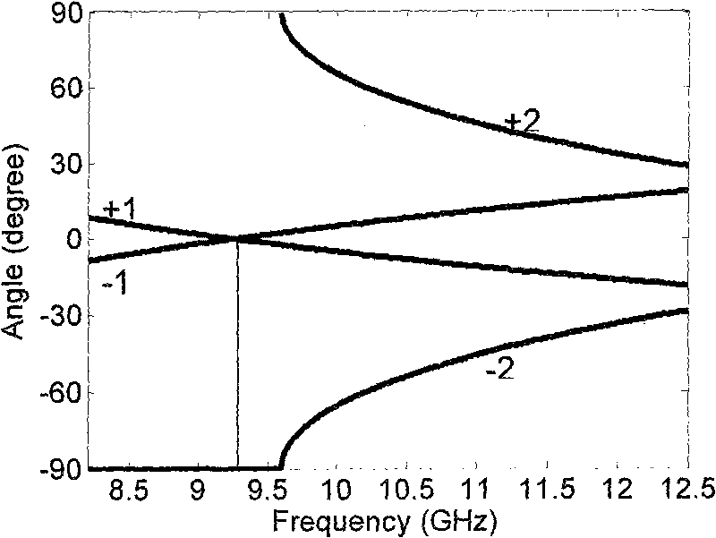
[0035] (2) The waveguide feed source is a flat rectangular waveguide BB100, and the width of the waveguide on the E plane is only 5.0mm. The frequency range of the radiation source is between 8.2GHz and 12.5GHz, and the corresponding wavelength range is 24mm to 36.6mm, and the wave vector k 0 0.17mm range -1 ~0.26mm -1 , in the microwave band;

[0036] (3) Select the period of type A groove as p30mm, which is equivalent to the radiation wavelength of the radiation source, the width w of type a groove is 5.0mm, and the depth l is 4.5mm;

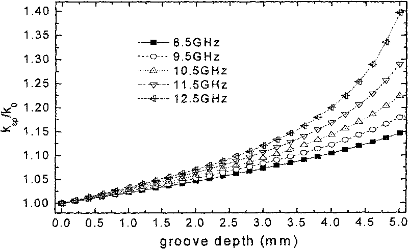
[0037] (4) The period d of the B-type groove is 2.38mm, the width a of the B-type groove is 1.2mm, and the adjustment law of the depth h to the wave vector of the surfac...


PUM

PropertyMeasurementUnit
widthaaaaaaaaaa
depthaaaaaaaaaa
thicknessaaaaaaaaaa

Abstract

The invention relates to a surface artificial electromagnetic material applied to directional radiation modulation. The material is manufactured by the following steps of: (1) selecting a base metal material; (2) determining the shape of a center feed source and the frequency band of a radiation source; (3) determining the period p, the width w and the groove depth l of a type-a groove to be manufactured; (4) determining the period d, the width a and the depth h of a type-b groove; and (5) manufacturing a period type-A groove and a period type-B groove on one side on a metal substrate so as to obtain the surface artificial electromagnetic material with directional radiation. The surface artificial electromagnetic material can realize the modulation of equivalent wave vectors of metal surface waves. Under the combined action of the type-A groove and the type-B groove, the surface artificial electromagnetic material can achieve the regulation and control on far-field radiation characteristics.

Description

technical field [0001] The invention designs an artificial electromagnetic material, especially a surface artificial electromagnetic material applied to antenna directional radiation modulation. Background technique [0002] In 2002, H.J.Lezec et al. discovered a strange phenomenon about the impact of subwavelength structures on electromagnetic energy radiation. They found that when a light wave passes through a small metal hole surrounded by subwavelength folds, the transmission direction of the transmitted beam can be very effectively controlled. W.L.Barnes spoke highly of the significance of the discovery. He believes that this sub-wavelength structured surface structure not only reveals the abnormal electromagnetic behavior of metal structures at a smaller scale, but also provides a new idea for the development of the next generation of integrated and miniaturized optical devices. The beam collimation characteristics also provide a convenient way for the development of...

Claims


Application Information

Patent Timeline
Patent Type & Authority Applications(China)
IPC IPC(8): H01F10/00H01F10/28H01Q15/00
Inventor 邓启凌史浩飞王义富袁桂山杜春雷
Owner INST OF OPTICS & ELECTRONICS - CHINESE ACAD OF SCI
Learn More