Supercharge Your Innovation With Domain-Expert AI Agents!

Through hole etching method

A technology of through-hole etching and etching stop layer, which is applied in the direction of electrical components, semiconductor/solid-state device manufacturing, circuits, etc., can solve the problems such as the inability to reduce the feature size of the through-hole and increase the cost.

Active Publication Date: 2010-06-09
SEMICONDUCTOR MANUFACTURING INTERNATIONAL (BEIJING) CORP
View PDF0 Cites 2 Cited by
  • Summary
  • Abstract
  • Description
  • Claims
  • Application Information

AI Technical Summary

Problems solved by technology

[0015] The currently etched via hole feature size is determined by the via hole size reserved by the patterned photoresist layer 70, such as Figure 1b As shown, as the size of the device decreases, the feature size of the via hole will also decrease, so when the photoresist layer 70 is patterned, using the existing exposure and development methods will result in reserved The via size is larger than the preset via feature size
For example, if figure 2 As shown, the set characteristic size of the through hole is 10 nanometers or 9 nanometers, but due to the limitations of the existing exposure and development methods, after patterning the photoresist layer 70, only 11 nanometers can be reserved. Hole size
In this way, the via hole feature size cannot be reduced without changing the existing exposure and development method, but changing the existing exposure and development method will increase the cost

Method used


Image

  • Through hole etching method
  • Through hole etching method
  • Through hole etching method

Examples


Embodiment Construction

[0033] In order to make the object, technical solution and advantages of the present invention clearer, the present invention will be further described in detail below with reference to the accompanying drawings and examples.

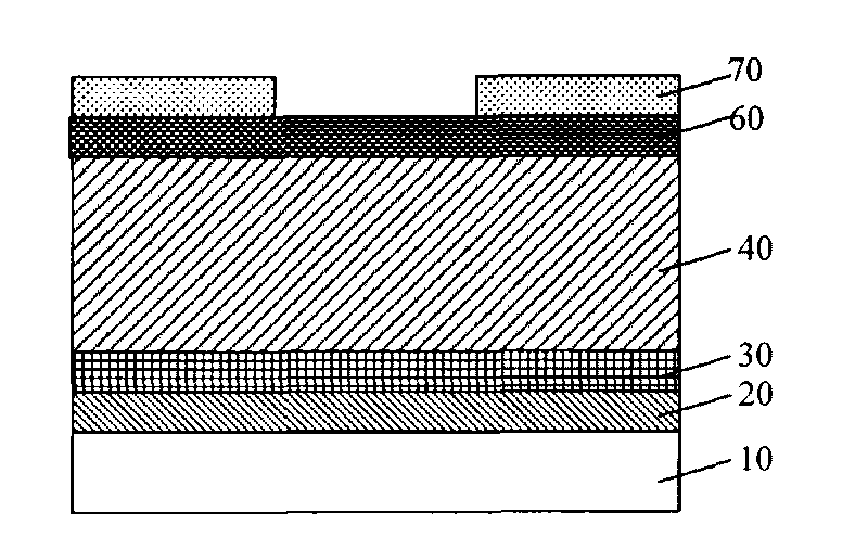
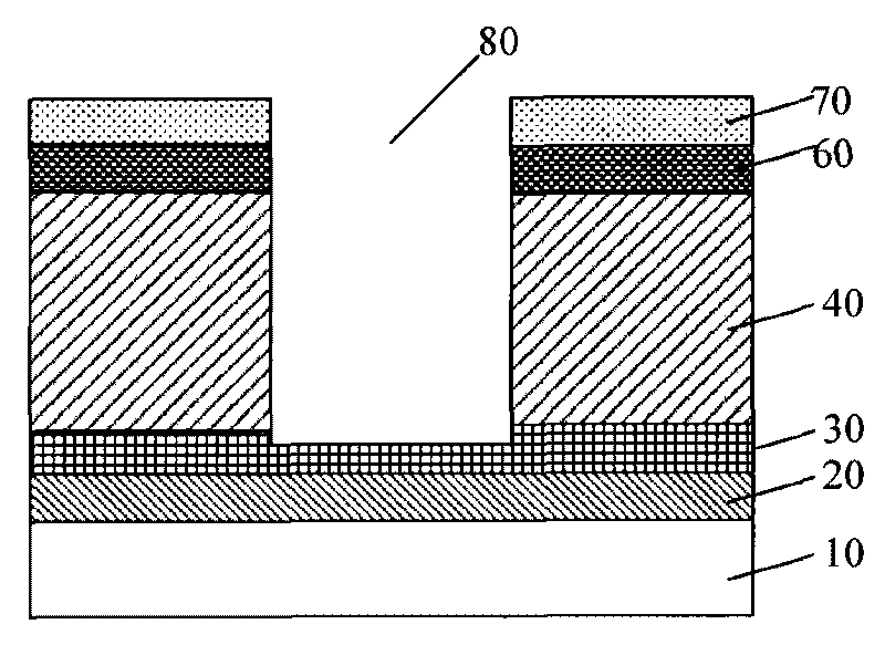
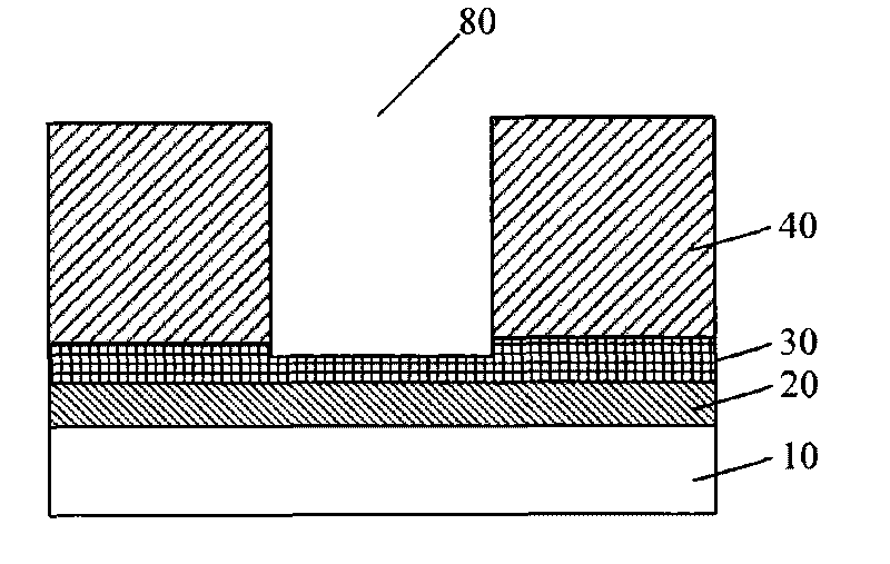
[0034] As described in the background art, in order to reduce the feature size of the via hole formed on the device, the pattern formed by the photoresist layer 70 can be precisely formed to ensure that the reserved via hole size is a set smaller feature size. In order to accurately form the pattern of the photoresist layer 70 , it is necessary to improve the exposure and development techniques of the prior art, which is not only difficult to achieve but also greatly increases the cost.

[0035] Therefore, in order not to change the existing exposure and development methods, the through hole obtained by etching can also reach the set relatively small through hole feature size, when the present invention uses HBr to etch the bottom anti-reflection coating...


PUM

PropertyMeasurementUnit
Thicknessaaaaaaaaaa

Abstract

The invention discloses a through hole etching method which etches a through hole after a through hole etching structure is formed; when a bottom anti-reflection coating in the through hole etching structure is etched, hydrogen bromide gas is adopted for etch to obtain a tapered hole structure. The through hole etching method can enable the characteristic dimension of the etched through hole to reach the required characteristic dimension of the through hole without changing the traditional exposure and developing method.

Description

technical field [0001] The invention relates to the technical field of semiconductor manufacturing, in particular to a through hole etching method. Background technique [0002] Vias play an important role in the composition of device structures as the interconnection between multilayer metal layers and the connection between the active area of ​​the device and the external circuit. In order to ensure the stability of the device operation, the through hole filled with conductive material is required to have good conductive characteristics, that is, the smaller the resistance value, the better, which makes it very important to strictly control the through hole etching process. [0003] With the increasing density of devices and complexity of processes, higher requirements are placed on the via etching process. The traditional via hole etching method uses an etching process to etch the stop layer (stop layer) once, which causes great damage to the via hole. With the developme...

Claims


Application Information

Patent Timeline
IPC IPC(8): H01L21/311H01L21/768
Inventor 张海洋陈海华黄怡赵林林
Owner SEMICONDUCTOR MANUFACTURING INTERNATIONAL (BEIJING) CORP
Features
  • R&D
  • Intellectual Property
  • Life Sciences
  • Materials
  • Tech Scout
  • Unparalleled Data Quality
  • Higher Quality Content
  • 60% Fewer Hallucinations
Learn More