Wide viewing angle LCD (Liquid Crystal Display) array substrate and manufacturing method thereof

A liquid crystal display and array substrate technology, applied in semiconductor/solid-state device manufacturing, instruments, electric solid-state devices, etc., can solve the problems of increased manufacturing cost, limited improvement of viewing angle, and difficult manufacturing process, so as to widen the viewing angle and simplify the structure and manufacturing process, the effect of a wide range of application prospects

Inactive Publication Date: 2010-06-16
BOE TECH GRP CO LTD
View PDF0 Cites 4 Cited by
  • Summary
  • Abstract
  • Description
  • Claims
  • Application Information

AI Technical Summary

Problems solved by technology

The TN+film mode has very limited improvement on the viewing angle. The viewing angle improvement is limited to the range of 140° horizontally and 100° vertically. It is generally only applied to notebook computers and desktop monitors, and is not suitable for large-size LCD TV applications; MVA mode requires A complex raised structure is manufactured on the side of the color filter substrate (color filter), which increases the manufacturing cost; the PVA mode requires the pixel electrode to be made into a complex slit structure, which affects the light utilization efficiency; while the IPS mode and the FFS mode High process control precision is required, and the manufacturing process is difficult

Method used


Image

  • Wide viewing angle LCD (Liquid Crystal Display) array substrate and manufacturing method thereof
  • Wide viewing angle LCD (Liquid Crystal Display) array substrate and manufacturing method thereof
  • Wide viewing angle LCD (Liquid Crystal Display) array substrate and manufacturing method thereof

Examples


Embodiment Construction

[0045] The technical solutions of the present invention will be described in further detail below with reference to the accompanying drawings and embodiments.

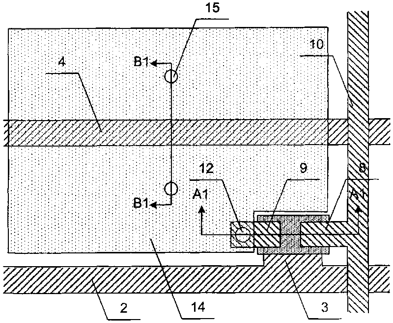
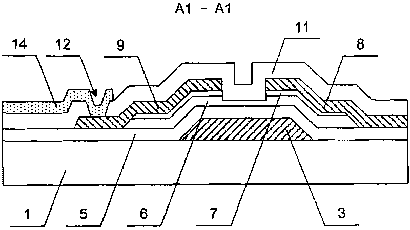
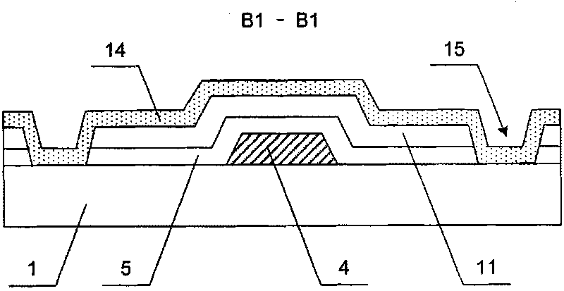
[0046] figure 1 It is a schematic structural view of the array substrate of the wide viewing angle liquid crystal display of the present invention, figure 2 for figure 1 The sectional view of A1-A1 direction in the middle, image 3 for figure 1 The cross-sectional view of B1-B1 in the middle. Such as Figure 1 ~ Figure 3As shown, the main structure of the array substrate of the wide viewing angle liquid crystal display of the present invention includes gate lines 2, data lines 10, pixel electrodes 14 and thin film transistors (Thin Film Transistor, TFT for short), and the gate lines 2 and data lines 10 together define the pixel area , the thin film transistor is formed at the intersection of the gate line 2 and the data line 10, the pixel electrode 14 is formed in the pixel area, and at least one vertical well 15...


PUM

PropertyMeasurementUnit
thicknessaaaaaaaaaa

Abstract

The invention relates to a wide viewing angle LCD array substrate and a manufacturing method thereof. The array substrate comprises a gating line and a data line which are formed on a substrate; a thin film transistor and a pixel electrode are formed in a pixel area limited by the grating line and the data line; and the pixel electrode is provided with at least one vertical shaft for inducing liquid crystal to form a multidomain structure. The manufacturing method comprises the following steps: forming patterns including the grating line, a gate electrode, the data line, a drain electrode and a TFT channel region; depositing a passivation layer which is provided with a first through hole for connecting the drain electrode and the pixel electrode and a second through hole for forming the vertical shaft; and depositing a transparent conductive film, forming a pattern including the pixel electrode in the pixel area, and forming the vertical shaft for inducing liquid crystal to form a multidomain structure at the second through hole. The wide viewing angle LCD array substrate utilizes the vertical shaft structure to induce liquid crystal to form the multidomain structure, thereby realizing a wide viewing angle with symmetrical viewing angles and simplifying the array substrate structure and the manufacturing process.

Description

technical field [0001] The invention relates to a liquid crystal display and a manufacturing method thereof, in particular to a wide viewing angle liquid crystal display array substrate and a manufacturing method thereof. Background technique [0002] The market of liquid crystal display is growing rapidly, and the application fields are continuously expanding, especially the application of large-size liquid crystal TV, which requires the liquid crystal display to have a wide range of viewing angles. The liquid crystal display includes an array substrate and a color filter substrate in a cell, and a liquid crystal is arranged between them. The liquid crystal is deflected under the action of voltage, and the degree of deflection of the liquid crystal can be controlled by controlling the magnitude of the voltage, so as to achieve the purpose of modulating the transmittance (display gray scale). [0003] Due to the defects of narrow viewing angles in existing liquid crystal di...

Claims


Application Information

Patent Timeline
Patent Type & Authority Applications(China)
IPC IPC(8): G02F1/1362G02F1/1343H01L21/84H01L27/12
CPCG02F1/13439G02F1/133707G02F1/133753H01L27/12G02F2001/133792H01L27/1214G02F1/133792H01L27/1288
Inventor 邵喜斌尹海军张俊瑞
Owner BOE TECH GRP CO LTD
Why Eureka
Try Eureka