Semiconductor solenoid inductor and manufacture method thereof

A manufacturing method and solenoid technology, applied in the field of inductance, can solve the problems of occupation, large chip area, inability to generate large magnetic induction intensity, etc., and achieve the effects of reducing chip area, improving integration, and improving magnetic induction intensity.

Inactive Publication Date: 2010-06-16
SHANGHAI HUA HONG NEC ELECTRONICS
View PDF0 Cites 3 Cited by
  • Summary
  • Abstract
  • Description
  • Claims
  • Application Information

AI Technical Summary

Problems solved by technology

At present, the commonly used production method is to use spiral coils, such as figure 1 As shown, since there is no magnetic core, this inductor cannot produce a large magnetic induction intensity, and in order to increase the magnetic induction intensity, it is necessary to increase the number

Method used


Image

  • Semiconductor solenoid inductor and manufacture method thereof
  • Semiconductor solenoid inductor and manufacture method thereof
  • Semiconductor solenoid inductor and manufacture method thereof

Examples


Example Embodiment

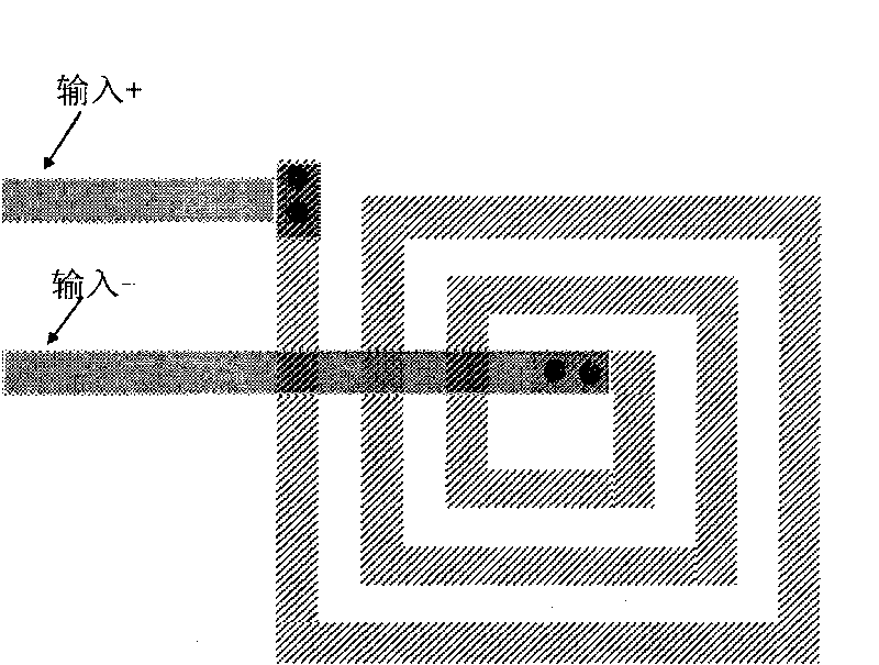
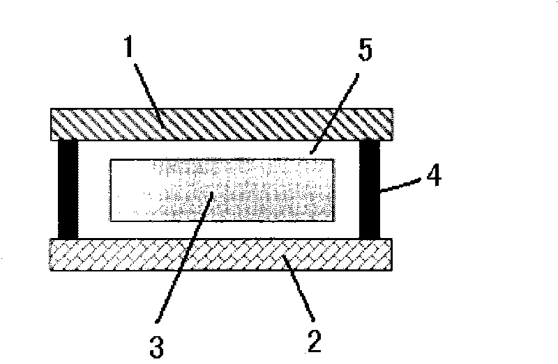
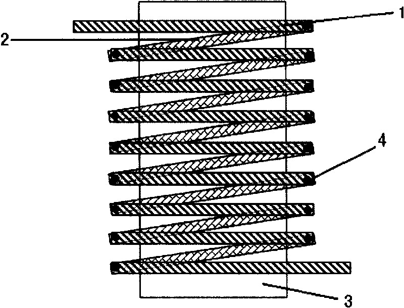
[0019] The invention discloses a semiconductor solenoid inductor, such as figure 2 , image 3 and Figure 4 As shown, it includes multiple upper metal strips 1 and multiple lower metal strips 2, a magnetic core 3 is sandwiched between the upper metal strip 1 and the lower metal strip 2, the upper metal strip 1 and the lower metal strip 2 The strips 2 are connected end to end in sequence through the contact holes 4 to form a solenoid that surrounds the magnetic core 3 in the same direction, and the magnetic core 3 is surrounded by an insulating medium 5 .

[0020] like image 3 As shown, the magnetic core is strip-shaped.

[0021] like Figure 4 As shown, the magnetic core is annular.

[0022] The invention also discloses a manufacturing method of the above-mentioned semiconductor solenoid inductor, which comprises the following steps in sequence:

[0023] (1) Photolithography and etching to form lower metal strips 2, such as Figure 5 shown;

[0024] (2) An insulating...


PUM


Abstract

The invention discloses a semiconductor solenoid inductor which comprises a plurality of upper-layer metal strips and a plurality of lower-layer metal strips, wherein a magnetic core is clamped between the upper-layer metal strips and the lower-layer metal strips; the upper-layer metal strips and the lower-layer metal strips are sequentially connected end to end by contact holes to form a solenoid surrounding the magnetic core along the same direction; the periphery of the magnetic core is wrapped by insulating medium. The invention also discloses a manufacture method of the semiconductor solenoid inductor, which comprises the following steps of: photoetching to form the lower-layer metal strips; then manufacturing an insulating layer on the lower-layer metal strips, manufacturing the magnetic core on the insulating layer and manufacturing an insulating layer on the magnetic core again; manufacturing the contact holes and leading the head ends and the tail ends of the lower-layer metal strips out; and finally photoetching on the insulating layer to form the upper-layer metal strips. The invention effectively improves the magnetic induction intensity in a way of the mutual connection and winding of the metal strips among different layers and the magnetic core, reduces the chip area occupied by a semiconductor inductor and improves the integrated level of chips.

Description

technical field [0001] The present invention relates to an inductor, in particular to a semiconductor solenoid inductor. The invention also relates to a manufacturing method of the semiconductor solenoid inductor. Background technique [0002] In the field of radio frequency integrated circuits or radio frequency micromachines, inductors are a commonly used device. At present, the commonly used production method is to use helical coils, such as figure 1 As shown, since there is no magnetic core, this inductance cannot generate a large magnetic induction intensity, and in order to increase the magnetic induction intensity, it is necessary to increase the number of turns of the coil as much as possible, but increasing the number of turns makes this inductance occupy a larger chip area. Now, the integration of semiconductor devices is getting higher and higher, and the existing semiconductor capacitors have become less and less able to meet the needs of technological developm...

Claims


Application Information

Patent Timeline
IPC IPC(8): H01F17/04H01F41/00H01L29/00H01L29/82
Inventor 陈华伦陈瑜熊涛罗啸陈雄斌
Owner SHANGHAI HUA HONG NEC ELECTRONICS
Why Eureka
Try Eureka