
Method for manufacturing alignment mark of semiconductor silicon wafer and semiconductor silicon wafer thereby

A silicon wafer alignment and manufacturing method technology, applied in semiconductor/solid-state device manufacturing, semiconductor devices, semiconductor/solid-state device components, etc., can solve the problem of insufficient use of cutting lanes, the influence of alignment signal morphology, signal strength, and quasi-marking Shape changes and other issues, to achieve the effect of saving the use of area

Inactive Publication Date: 2010-06-16
SHANGHAI HUA HONG NEC ELECTRONICS
View PDF0 Cites 3 Cited by
  • Summary
  • Abstract
  • Description
  • Claims
  • Application Information

AI Technical Summary

Problems solved by technology

Especially in the development of new processes, it is often necessary to add many batches of alignment marks for evaluation. At this time, the dicing lanes are often not enough
Simultaneously, because the chip size of the silicon chip of the new product that develops every time is different, need rearrange the position of alignment mark every time; profile) and signal strength will be affected
[0003] In addition, in various processes of semiconductors, the morphology of alignment marks may change due to various reasons
like figure 1 As shown, when the shape of the alignment mark changes, a secondary peak may be introduced, resulting in distortion of the alignment signal, thereby affecting the coordinates of the alignment mark

Method used


Image

  • Method for manufacturing alignment mark of semiconductor silicon wafer and semiconductor silicon wafer thereby
  • Method for manufacturing alignment mark of semiconductor silicon wafer and semiconductor silicon wafer thereby
  • Method for manufacturing alignment mark of semiconductor silicon wafer and semiconductor silicon wafer thereby

Examples


Embodiment Construction

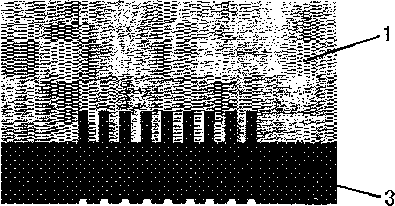
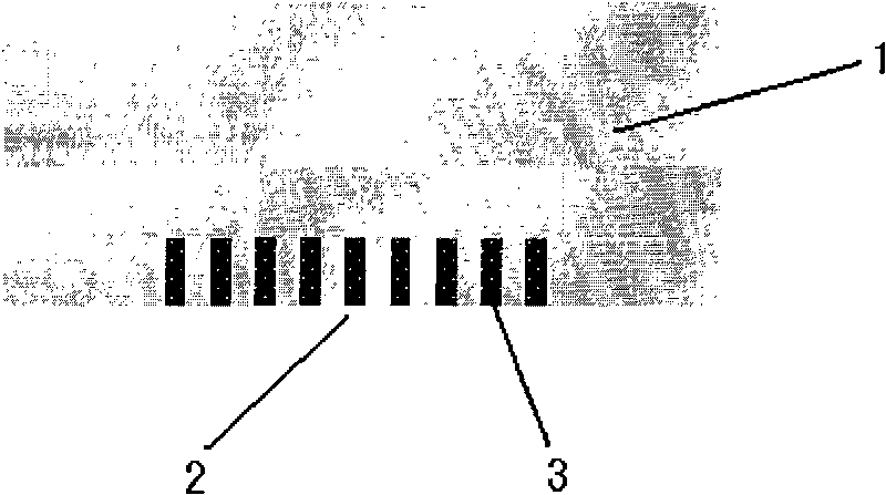
[0015] The invention discloses a method for manufacturing an alignment mark on a semiconductor silicon wafer, such as figure 2 As shown, before photolithography, a layer of luminescent material 3 is deposited on the back of the semiconductor silicon wafer 1, then photolithography is performed on the back of the silicon wafer, and the luminescent material layer is etched in the subsequent etching step to form Alignment mark 2, such as image 3 shown.

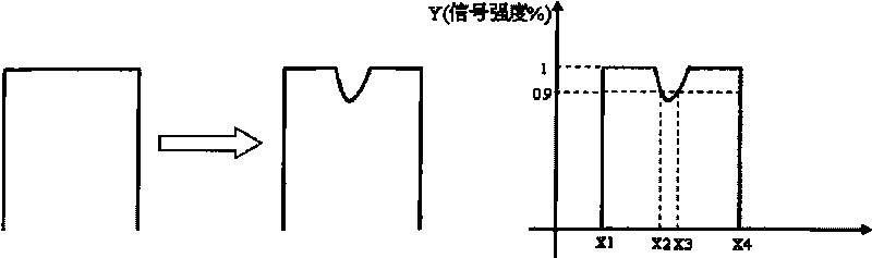
[0016] In the present invention, the alignment mark is made of luminescent material. The luminescent substance is added to the alignment mark, which greatly enhances the signal intensity of the peak. In this way, even if the bottom shape of the alignment mark is not good or there are residues, the signal intensity can be improved and the signal intensity can be reduced. Measurement error. Such as Figure 4 As shown, when the alignment mark is doped with a luminescent substance, the signal intensity of the alignment mark is m...


PUM


Abstract

The invention discloses a method for manufacturing an alignment mark of a semiconductor silicon wafer. The method comprises the following steps of: depositing a layer of luminescent material on the back face of the semiconductor wafer, photoetching the back of the semiconductor wafer, manufacturing the alignment mark through corrosion and removing photoresist. The invention also discloses a semiconductor wafer, the back of the semiconductor wafer is provided with the alignment mark which is made of the luminescent material. In the invention, the alignment mark is arranged on the back of the semiconductor wafer, thereby the use area of the front of the wafer is greatly saved. The position of the alignment mark is fixed so that an alignment signal can not be influenced by different products and different processes.

Description

technical field [0001] The invention relates to a method for manufacturing an alignment mark of a semiconductor silicon wafer. The invention also relates to a semiconductor silicon wafer. Background technique [0002] Currently, in semiconductor manufacturing, alignment marks are placed in the dicing lanes on the front side of the silicon wafer, thus reducing the area used on the front side of the silicon wafer. Especially in the development of a new process, it is often necessary to add many batches of alignment marks for evaluation. At this time, the dicing lanes are often not enough. Simultaneously, because the chip size of the silicon chip of the new product that develops every time is different, need rearrange the position of alignment mark every time; profile) and signal strength will be affected. [0003] In addition, in various processes of semiconductors, the morphology of the alignment marks may change due to various reasons. Such as figure 1 As shown, when th...

Claims


Application Information

Patent Timeline
IPC IPC(8): H01L21/00H01L23/544
Inventor 陈福成
Owner SHANGHAI HUA HONG NEC ELECTRONICS
Features
  • Generate Ideas
  • Intellectual Property
  • Life Sciences
  • Materials
  • Tech Scout
  • Unparalleled Data Quality
  • Higher Quality Content
  • 60% Fewer Hallucinations
Learn More