
Quad flat no-lead encapsulation structure and encapsulation method thereof

A technology of leadless packaging and packaging method, which is applied in the manufacturing of electrical components, electric solid-state devices, semiconductor/solid-state devices, etc., can solve the degradation of pin insulation performance, the deterioration of conductive pin insulation properties, and limit the application of QFN packaging technology. field and other issues, to achieve the effect of improving insulation properties

Active Publication Date: 2010-06-16
DIODES SHANGHAI
View PDF0 Cites 6 Cited by
  • Summary
  • Abstract
  • Description
  • Claims
  • Application Information

AI Technical Summary

Problems solved by technology

[0005] In the prior art, although the heat sink in the packaging structure of the QFN package is conducive to the heat dissipation of the chip to the outside during the working process, it leads to the deterioration of the insulation properties between the conductive pins of the package.
For chips with low heat generation, users often prefer good insulation performance between the conductive pins of the package. seems redundant
For the current QFN process, the bottom of the package must have an exposed conductive heat sink, which limits the application field of the QFN packaging process.

Method used


Image

  • Quad flat no-lead encapsulation structure and encapsulation method thereof
  • Quad flat no-lead encapsulation structure and encapsulation method thereof
  • Quad flat no-lead encapsulation structure and encapsulation method thereof

Examples


Embodiment Construction

[0019] The specific implementation of a quadrilateral flat no-lead package structure and its packaging method provided by the present invention will be described in detail below with reference to the accompanying drawings.

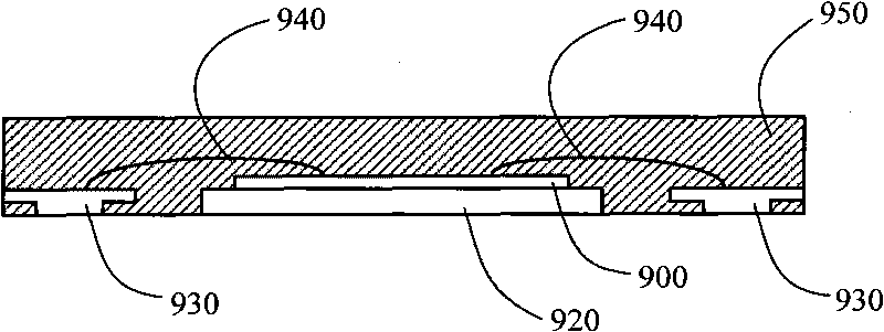
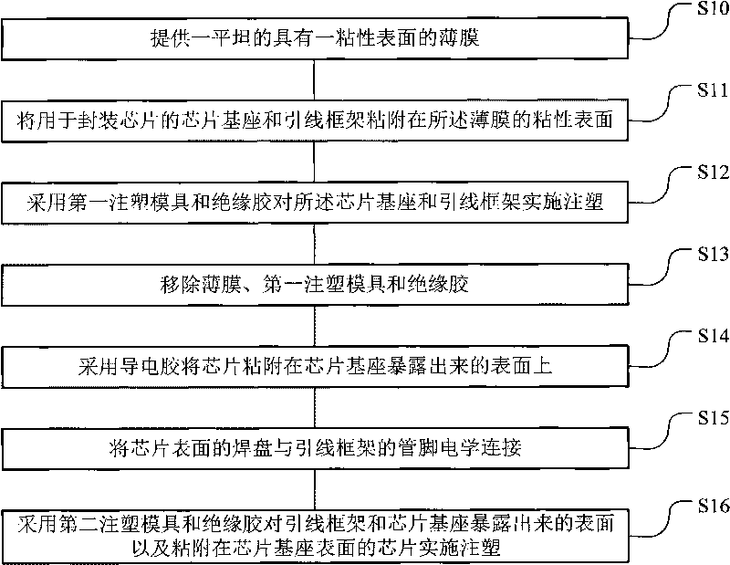
[0020] attached figure 2 In the shown specific embodiment of the present invention, the schematic diagram of the implementation steps of the packaging method includes the following steps: step S10, providing a flat film with an adhesive surface; step S11, using the chip base and the lead frame for packaging the chip Adhering to the sticky surface of the film; Step S12, using the first injection mold and insulating glue to inject the chip base and lead frame; Step S13, removing the film, the first injection mold and insulating glue; Step S14 , using conductive glue to adhere the chip on the exposed surface of the chip base; step S15, electrically connecting the pads on the chip surface with the pins of the lead frame; step S16, using the second injection m...


PUM


Abstract

The invention provides an encapsulation method of a quad flat no-lead encapsulation structure. The encapsulation method comprises the following steps: providing a flat film with a viscous surface; adhering a chip base and a lead frame which are used for encapsulating a chip to the viscous surface of the film; performing injection molding on the chip base and the lead frame by using a first injection mould and insulation adhesive; removing the film, the first injection mould and the insulation adhesive; adhering the chip to the exposed surface of the chip base by using conductive adhesive; electrically connecting pads on the surface of the chip with a base pin of the lead frame; and performing injection molding by using a second injection mould and the insulation adhesive. The invention further provides the quad flat no-lead encapsulation structure obtained by the method of the invention. The invention has the advantage that the chip base can be ensured to be completely covered by the insulation adhesive and can not be exposed in the follow-up processes, thus increasing the insulation property between pads.

Description

【Technical field】 [0001] The invention relates to the field of semiconductor packaging, in particular to a quadrilateral flat leadless packaging structure and a packaging method thereof. 【Background technique】 [0002] With the rapid development of electronic manufacturing technology, consumer electronic products are becoming more and more small and portable, which also leads to an increasingly limited space for arranging electrical components inside these electronic products. In this case, the electrical components used must be as thin as possible, which has become the current development trend of electronic component manufacturing. The quad flat no-leads (QFN) process can just meet this demand. [0003] attached figure 1 Shown is a schematic cross-sectional view of a typical QFN package structure in the prior art, including a chip 900 , a heat sink 920 , a lead frame 930 , multiple wires 940 , and insulating glue 950 wrapping the above structure. The chip 900 is adhered...

Claims


Application Information

Patent Timeline
IPC IPC(8): H01L21/50H01L21/56H01L23/12H01L23/31
CPCH01L2224/45124H01L2224/73265H01L2224/32245H01L2224/48247H01L24/73
Inventor 李志宁柳丹娜
Owner DIODES SHANGHAI
Features
  • Generate Ideas
  • Intellectual Property
  • Life Sciences
  • Materials
  • Tech Scout
  • Unparalleled Data Quality
  • Higher Quality Content
  • 60% Fewer Hallucinations
Learn More