Semiconductor device and method of manufacturing same

A semiconductor and heating element technology, which is applied in semiconductor devices, electric solid devices, electrical components, etc., can solve the problems of phase change memory device performance reduction, heating element energy loss, etc., to improve heat insulation properties and reduce reset current. Effect

Active Publication Date: 2011-11-09
TAIWAN SEMICON MFG CO LTD
View PDF5 Cites 8 Cited by
  • Summary
  • Abstract
  • Description
  • Claims
  • Application Information

AI Technical Summary

Problems solved by technology

However, one of the obstacles to the development of phase change memory devices is the energy

Method used


Image

  • Semiconductor device and method of manufacturing same
  • Semiconductor device and method of manufacturing same
  • Semiconductor device and method of manufacturing same

Examples


Example Embodiment

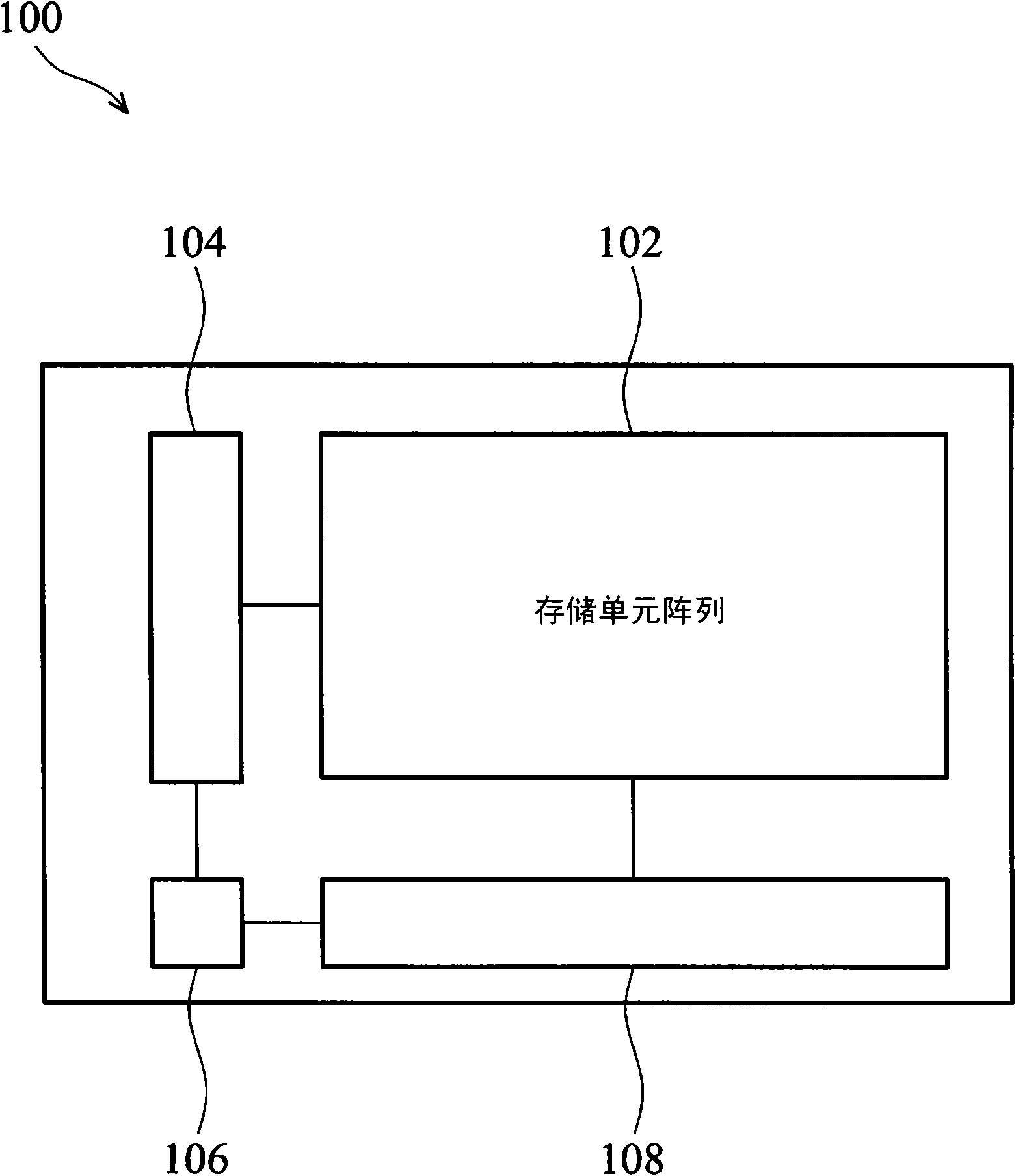
[0064] The present invention relates to a semiconductor device, and more particularly to a memory device with elements in an array or peripheral area and its manufacturing method. However, the embodiments provided here are used for teaching the scope of the invention. Those skilled in the art can easily understand the technology and other methods and systems disclosed in the present invention, and the methods and systems disclosed in the present invention also include some general structures and and / or steps, since these structures and steps are already known, they will only be roughly described.

[0065] In addition, the partially repeated numbers in the drawings are for convenience of description, and do not mean that any combination of methods or devices is required in the drawings. In addition, the following will describe the situation where the first feature is formed on, adjacent to, adjacent to, or connected to the second feature, which may include the implementation of...


PUM


Abstract

The invention provides a semiconductor device and a method of manufacturing the same. The semiconductor device is provided which includes a bottom electrode contact formed on a substrate, and a dielectric layer formed on the bottom electrode contact. The device further includes a heating element formed in the dielectric layer, wherein the heating element is disposed between two air gaps separating the heating element from the dielectric layer, and a phase change element formed on the heating element, wherein the phase change element includes a substantially amorphous background and an active region, the active region capable of changing phase between amorphous and crystalline. The invention can improve the heat insulation property of the phase change element and effectively decrease a reset curren that is required to form the phase of the active region to the amorphous state.

Description

technical field [0001] The present invention relates to a semiconductor device, and in particular to a semiconductor device with a phase change memory. Background technique [0002] An integrated circuit forms one or more elements on a semiconductor substrate by a process. With the improvement of technology and materials, the size of semiconductor components continues to shrink. However, the reduction in size of semiconductor devices encounters many problems to be overcome. [0003] Generally, phase change materials used in memory devices include two phases (or states): an amorphous phase and a crystalline phase. Amorphous phase materials generally have higher resistance values ​​than crystalline phase materials. The phase exhibited by the phase change material can be selectively changed by a stimulus (such as an electrical stimulus). The electrical stimulation method mentioned above can be, for example, applying a certain amount of current to the phase change material v...

Claims


Application Information

Patent Timeline
IPC IPC(8): H01L27/24H01L45/00
CPCH01L45/1233H01L45/144H01L45/06H01L45/16H01L45/1293H01L45/126H10N70/8413H10N70/8616H10N70/231H10N70/011H10N70/8828H10N70/826
Inventor 沈明辉刘世昌蔡嘉雄
Owner TAIWAN SEMICON MFG CO LTD
Why Eureka
Try Eureka