Method for forming interconnection line in semiconductor device

A technology of interconnection wires and semiconductors, which is applied in semiconductor/solid-state device manufacturing, electrical components, circuits, etc., can solve the problems of huge investment in research and development costs, and achieve the effect of reducing the generation of holes and reducing the reaction speed

Inactive Publication Date: 2010-06-16
SEMICONDUCTOR MANUFACTURING INTERNATIONAL (BEIJING) CORP
View PDF1 Cites 4 Cited by
  • Summary
  • Abstract
  • Description
  • Claims
  • Application Information

AI Technical Summary

Problems solved by technology

[0007] However, when the method provided in the above-mentioned patent application is used to reduce the generation of the holes, the step of forming the stress release layer needs to be introduced in the manufacturing process, and a new technology needs to be added to the original process, for example, the stress release layer needs to be explored. The formation process, and the degree of integration of the formation process with the existing process; requires huge research and development costs

Method used


Image

  • Method for forming interconnection line in semiconductor device
  • Method for forming interconnection line in semiconductor device
  • Method for forming interconnection line in semiconductor device

Examples


no. 1 example

[0031] As a first embodiment of the present invention, the step of forming interconnection lines in a semiconductor device includes:

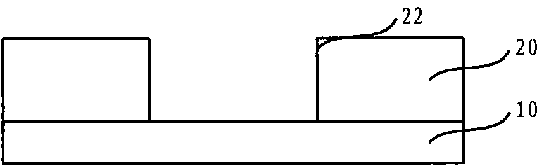
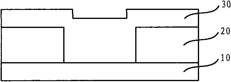
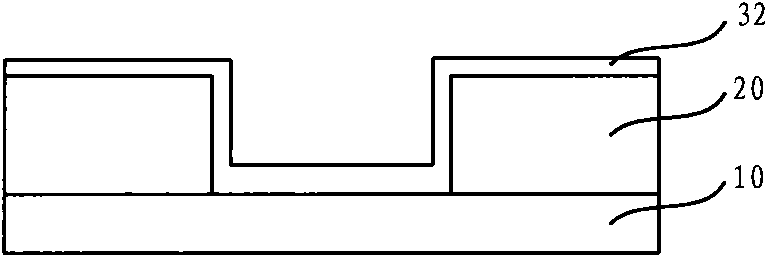
[0032] First, like Figure 7 As shown, a dielectric layer 120 having an interconnect structure 122 and a seed layer (not shown) covering the bottom and sidewalls of the interconnect structure 122 are formed on the substrate 100;

[0033] After defining the active region of the device on the substrate and completing the shallow trench isolation, and then forming the gate structure and the source and drain regions, the base 100 is formed. In addition, after defining the active area of ​​the device on the substrate and completing the shallow trench isolation, and then forming the gate structure and the source and drain regions, the first interlayer dielectric layer (ie, the pre-metal dielectric layer, PMD) is then deposited, and continue After the first layer interconnection line is formed in the first interlayer dielectric layer, the substrate 100 can...


PUM


Abstract

The invention relates to a method for forming an interconnection line in a semiconductor device, comprising the following steps of: forming a medium layer with an interconnection line structure and a seed crystal layer covering the bottom wall and the side wall of the interconnection line structure on a substrate; forming a bottom electroplating branch layer covering the seed crystal layer by adopting first current; forming a top electroplating branch layer covering the bottom electroplating branch layer and filling the interconnection line structure; the step of forming the top electroplating branch layer comprises the following step of: forming a transition electroplating branch layer covering the bottom electroplating branch layer by adopting transition current, wherein the transition current is between the first current and second current, and the second current enables the speed of forming a subsequent electroplating branch layer top layer to be higher than that of forming the bottom electroplating branch layer by adopting the first current; and forming an electroplating branch layer top layer covering the transition electroplating branch layer by adopting the second current. The invention can reduce hole generation in the electroplating process.

Description

Technical field [0001] The present invention relates to the technical field of semiconductor manufacturing, in particular to a method for forming interconnections in semiconductor devices. Background technique [0002] In the semiconductor manufacturing process, metal connection wires (referred to as interconnect wires in this document) are usually used to realize electrical connection between devices and external circuits. The step of forming the interconnection line includes: figure 1 As shown, a dielectric layer 20 having an interconnect structure 22 and a seed layer (not shown) covering the bottom and side walls of the interconnect structure 22 are formed on the substrate 10; figure 2 As shown, an electroplating layer 30 filling the interconnect structure 22 is formed on the seed layer. [0003] The basic principle of forming the electroplating layer 30 is that the substrate carrying the seed layer is immersed in an electroplating solution, and the substrate and the seed layer...

Claims


Application Information

Patent Timeline
Patent Type & Authority Applications(China)
IPC IPC(8): H01L21/768
Inventor 聂佳相康芸杨瑞鹏
Owner SEMICONDUCTOR MANUFACTURING INTERNATIONAL (BEIJING) CORP
Why Eureka
Try Eureka