

GGNMOS (grounded-gate negative-channel metal oxide semiconductor) device and making method thereof
A manufacturing method and device technology, applied in the direction of semiconductor/solid-state device manufacturing, semiconductor devices, electrical components, etc., can solve problems such as affecting ESD discharge capability, reducing the slope of the conduction curve, and increasing the device area to improve the triggering effect. , The effect of saving chip area and reducing the concentration of P well
- Summary
- Abstract
- Description
- Claims
- Application Information
AI Technical Summary
Problems solved by technology
Method used
Image

Examples
Embodiment Construction
[0030] The manufacturing method of GGNMOS device described in the present invention, comprises the steps:
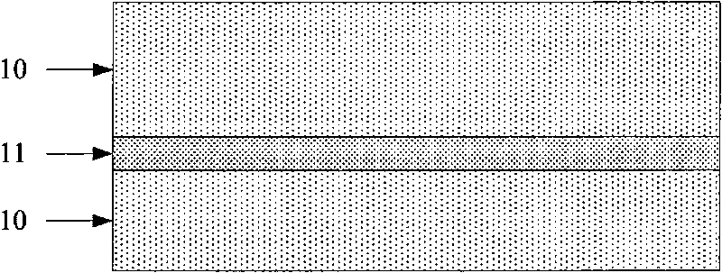
[0031] Step 1, see Figure 1a . N-type impurities are implanted on the P-type silicon substrate 10 by an ion implantation process to form a deep N well 11 . Commonly used N-type impurities are phosphorus, arsenic and antimony. Annealed in a high temperature furnace after ion implantation.
[0032] For example, the dose of ion-implanted phosphorus is 5×10 12 ions / cm 2 (ion per square centimeter) ~ 1.5×10 13 ions / cm 2 , the implantation energy is 1000keV-2000keV. The temperature of the high temperature furnace annealing is 1100° C. to 1200° C., and the time is 1 to 3 hours.
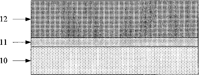
[0033] Step 2, see Figure 1b . P-type impurities are implanted on the P-type silicon substrate 10 by an ion implantation process, and the range of ion implantation is all silicon above the deep N well 11 , thereby forming a P well 12 on the deep N well 11 . Commonly used P-type impurities ...
PUM
 Abstract
Description
Claims
Application Information