High-capacity BCD technique for twice etching single/poly-silicon

A single-layer polysilicon, high-power technology, which is applied in the field of electronics, can solve the problem that the gate oxide is easily damaged, and achieve the effects of easy process implementation, avoiding the penetration of gate oxide into the channel region, and stable device performance

Inactive Publication Date: 2010-11-17
UNIV OF ELECTRONICS SCI & TECH OF CHINA
View PDF0 Cites 0 Cited by
  • Summary
  • Abstract
  • Description
  • Claims
  • Application Information

AI Technical Summary

Problems solved by technology

The present invention adopts the method of depositing polysilicon once, etching polysilicon twice and performing polysilicon doping to avoid the influence of doping ions in polysilicon on the gate oxide and channel region in the high temperature process of the polysilicon follow-up process, and solve the problem of the thermal process. The Problem of Gate Oxide Vulnerability

Method used


Image

  • High-capacity BCD technique for twice etching single/poly-silicon
  • High-capacity BCD technique for twice etching single/poly-silicon
  • High-capacity BCD technique for twice etching single/poly-silicon

Examples


Embodiment Construction

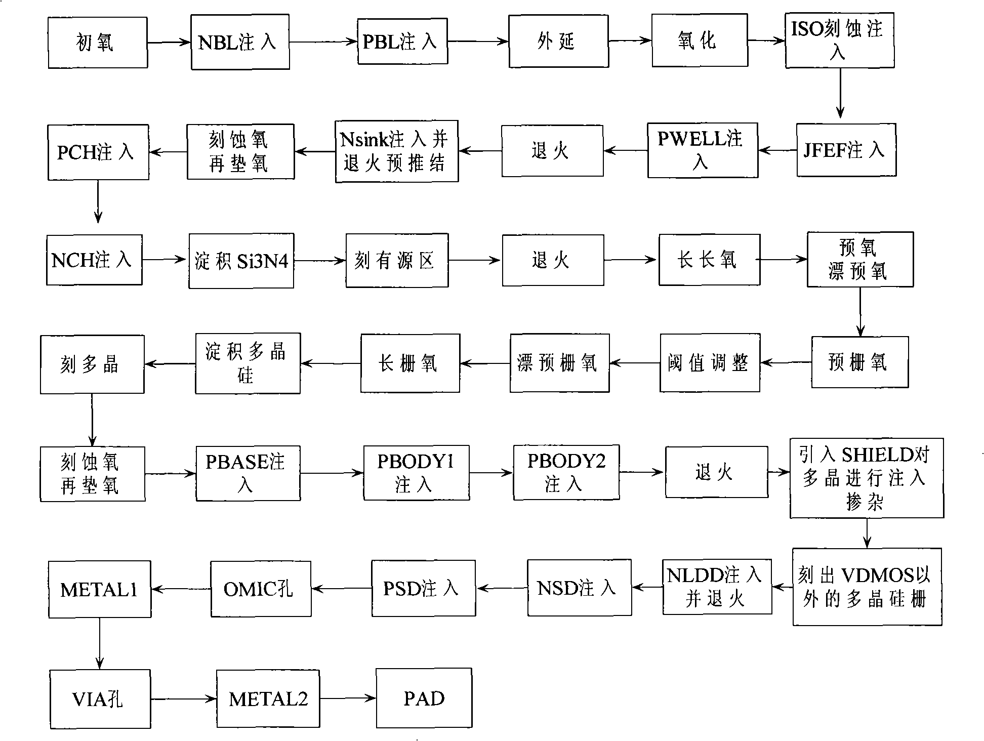
[0057] Specific examples of the present invention will be described below in conjunction with specific device structure diagrams.

[0058] figure 1 It is a concrete process flow diagram of the present invention, with reference to Figure 14 , this process can integrate high-voltage VDMOS, high-voltage PMOS, high-voltage NPN, high-voltage PNP, low-voltage NPN, substrate PNP, lateral PNP, low-voltage NMOS, low-voltage PMOS, low-voltage diodes, high-voltage diodes, Zener diodes, and various capacitors and resistors Various devices. refer to figure 1 , the specific process examples of the present invention include the following specific process steps.

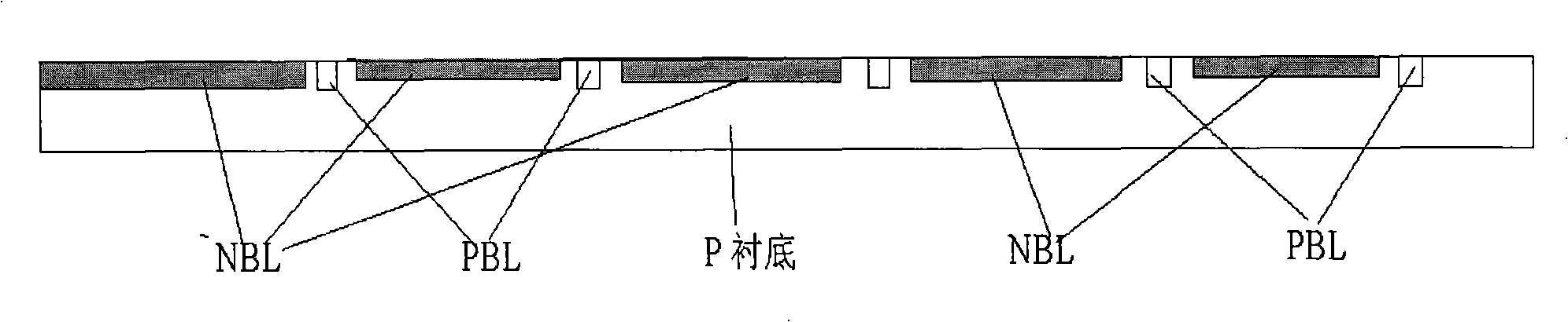
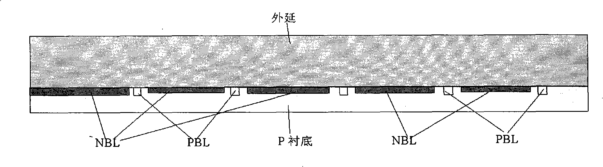
[0059] 1. Select the required substrate, here we choose the substrate with P-type crystal plane, and make alignment marks. The specific process steps include: initial oxygen formation of an oxide layer of about 1 μm; use photoresist to locate the buried layer region NBL, and then etch the oxide layer; grow a layer of particle-...


PUM


Abstract

The invention relates to a highly-efficient BCD technique of twice etching single polycrystalline silicon, belonging to the technical field of semiconductor components and integrated circuits. The invention in particular relates to a BCD component producing method which comprises the procedures of substrate pre-oxidization, NBL and PBL; epitaxial growth; ISO; Nsink; PCH and NCH injection; gate oxide layer growth; boron injection in PBASE, PBODY1 and PBODY2 regions; polycrystalline silicon doping; etching a polycrystalline silicon other than VDMOS; NLDD; NSD, PSD, etc. The invention adopts themethod of once depositing the polycrystalline silicon, twice etching the polycrystalline silicon and then doping the polycrystalline silicon to avoid the impact of doped ions in the polycrystalline silicon upon the gate oxide and a channel region during a high temperature process of a sequential polycrystalline process and to solve the problem that gate oxide is easy to be damaged during the heattreatment. A plurality of components such as a high voltage VDMOS, a high voltage PMOS, a high voltage NPN, a high voltage PNP, a low voltage NPN, a substrate PNP, a transverse PNP, a low voltage NMOS, a low voltage PMOS, a low voltage diode, a high voltage diode, a zener diode and compactors and resistors of various types can be integrated on a single chip. The technique has the advantages of high power, a great many integrated components, easy realization of the process, stable performance of components and good compatibility.

Description

technical field [0001] The invention belongs to the field of electronic technology, relates to a semiconductor device and an integrated circuit, and in particular to a manufacturing method of a BCD (Bipolar, CMOS, DMOS) device. Background technique [0002] The BCD process is a monolithic integration process technology that can manufacture Bipolar, CMOS and DMOS devices on the same chip, referred to as the BCD process. Since the BCD process combines the respective advantages of the above three devices, BCD-based products can integrate complex control functions, making it the mainstream process technology for power integrated circuits. For the BCD process, different devices can be selected for different circuits to optimize the corresponding sub-circuits, and realize the requirements of low power consumption, high integration, high speed, high driving capability, and high current of the entire circuit. [0003] This technology provides an ideal design platform for designing ...

Claims


Application Information

Patent Timeline
Patent Type & Authority Patents(China)
IPC IPC(8): H01L21/8249
Inventor 方健毛焜刘哲张弦王凯尹德阳王亮亮薛方俊罗波关旭张波
Owner UNIV OF ELECTRONICS SCI & TECH OF CHINA
Why Eureka
Try Eureka