Magnetic auxiliary laser patterning Micro-LED mass transfer method

An auxiliary laser and transfer method technology, which is applied in the direction of electrical components, circuits, semiconductor devices, etc., can solve the problems of long transfer cycle, low product reliability, and damage to Micro-LED chips, so as to achieve high applicability and avoid transfer failure Control and avoid the effect of mura

Pending Publication Date: 2021-10-29
NO 55 INST CHINA ELECTRONIC SCI & TECHNOLOGYGROUP CO LTD
View PDF5 Cites 2 Cited by
  • Summary
  • Abstract
  • Description
  • Claims
  • Application Information

AI Technical Summary

Problems solved by technology

Among them, the stamp transfer method realizes the transfer between different substrates through different adhesive forces of glue, such as the mass transfer equipment of Toray Precision Machinery Co., Ltd. This method has high alignment accuracy, but the adhesive force will cause damage to the Micro-LED chip , leading to low product reliability
Liquid phase transfer method and electrostatic transfer method can avoid this situation, but due to the uncontrolled transfer process, the transfer cycle is longer

Method used


Image

  • Magnetic auxiliary laser patterning Micro-LED mass transfer method
  • Magnetic auxiliary laser patterning Micro-LED mass transfer method

Examples


Embodiment Construction

[0027] The technical solutions of the present invention will be described in detail below in conjunction with the accompanying drawings.

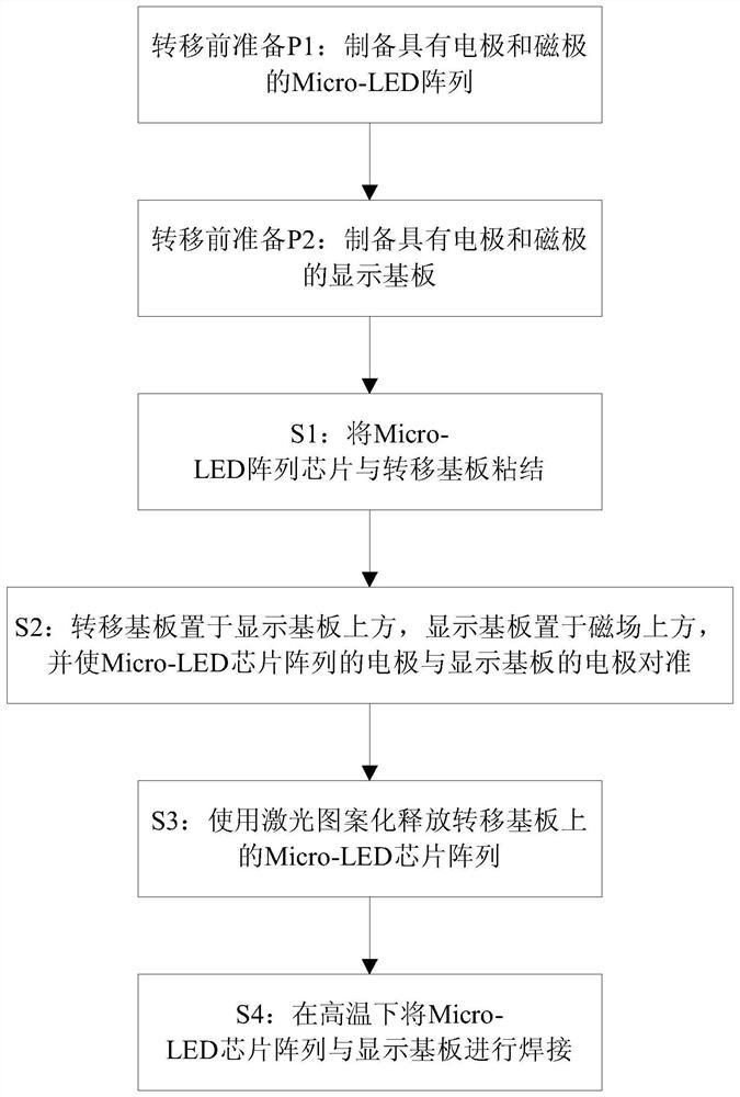
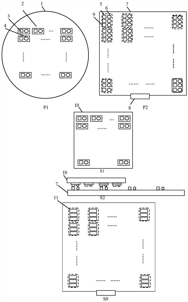
[0028] The present invention designs a magnetically assisted laser patterned Micro-LED mass transfer method, which prepares the transfer substrate of the Micro-LED array with electrodes and magnetic poles and prepares the display panel with corresponding electrodes and magnetic poles, and releases the glue by heating the laser The layer reduces the adhesive force of the adhesive layer, and the transfer of the Micro-LED array to the display substrate is realized with the assistance of the magnetic force at the corresponding position. The subsequent interconnection between the Micro-LED array and the display substrate is realized by heating, pressing, etc., which can be efficiently and accurately Transfer Micro-LEDs. The basic steps are as figure 1 shown.

[0029] Preparation before transfer P1: Prepare the Micro-LED array with electrodes a...


PUM


Abstract

The invention discloses a magnetic auxiliary laser patterning Micro-LED mass transfer method. The method comprises the following steps of bonding a Micro-LED chip array with a transfer substrate; placing the transfer substrate above a display substrate, placing the display substrate above a magnetic field, aligning the electrode of the Micro-LED chip array with the electrode of the display substrate, and adjusting the vertical distance between the transfer substrate and the display substrate; releasing the Micro-LED chip array on the transfer substrate through laser patterning, and aligning the Micro-LED array chip accurately with the display substrate under the action of the magnetic field; and welding the Micro-LED chip array and the display substrate at a high temperature. According to the method, the adhesive force of an adhesive layer is reduced through laser, and by adopting the patterning active transfer, the stress damage of a stamp transfer method to the Micro-LED and the transfer uncontrollability of a liquid phase transfer method and an electrostatic transfer method are avoided.

Description

technical field [0001] The invention belongs to the field of Micro-LED technology, and in particular relates to a Micro-LED mass transfer method. Background technique [0002] Micro-LED (Micro-LED) chips are LED epitaxial wafers etched into micron-scale and nano-scale LEDs, so that Micro-LEDs can directly emit light for display purposes. In the field of Micro-LED display, mass transfer technology is the difficulty of this technology. [0003] At present, the mass transfer technology of Micro-LED display mainly adopts the stamp (Stamp) transfer method, wafer para-position transfer method, liquid phase transfer method and electrostatic transfer method. Among them, the stamp transfer method realizes the transfer between different substrates through different adhesive forces of glue, such as the mass transfer equipment of Toray Precision Machinery Co., Ltd. This method has high alignment accuracy, but the adhesive force will cause damage to the Micro-LED chip , leading to low ...

Claims


Application Information

Patent Timeline
IPC IPC(8): H01L33/00H01L21/67H01L33/62
CPCH01L21/67144H01L33/0093H01L33/62
Inventor 杜正婷王进杨洪宝胡亮李晓剑刘凯丽王璐赵红伟张伟陈建军樊卫华
Owner NO 55 INST CHINA ELECTRONIC SCI & TECHNOLOGYGROUP CO LTD
Why Eureka
Try Eureka