Metal-semiconductor field effect transistor

A field effect transistor, metal semiconductor technology, applied in the field of semiconductor device manufacturing, can solve problems such as obvious leakage current, and achieve the effect of preventing leakage current

Active Publication Date: 2010-06-16
SEMICON MFG INT (SHANGHAI) CORP
View PDF1 Cites 12 Cited by
  • Summary
  • Abstract
  • Description
  • Claims
  • Application Information

AI Technical Summary

Problems solved by technology

[0004] The MESFET with the above structure will generate leakage current, especially when the size of semiconductor devices becomes smaller and smaller, this leakage current becomes more and more obvious

Method used


Image

  • Metal-semiconductor field effect transistor
  • Metal-semiconductor field effect transistor
  • Metal-semiconductor field effect transistor

Examples


Embodiment Construction

[0024] The specific content of the present invention will be described in detail below in conjunction with the accompanying drawings.

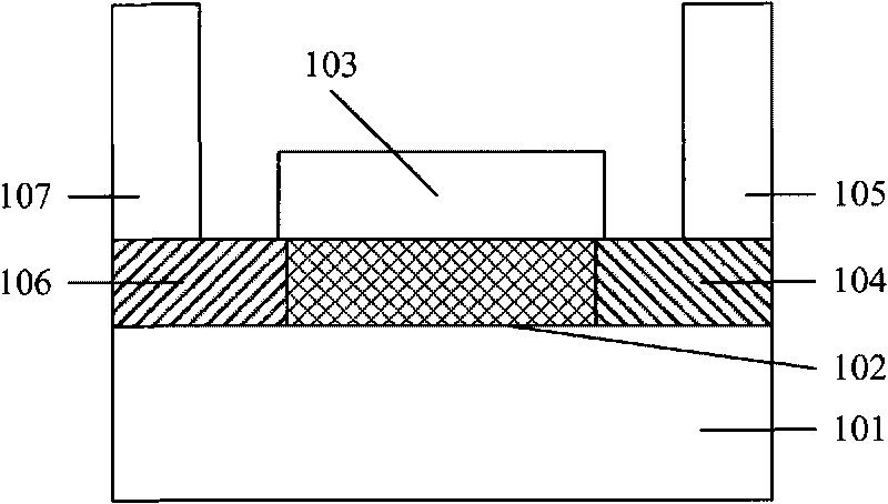
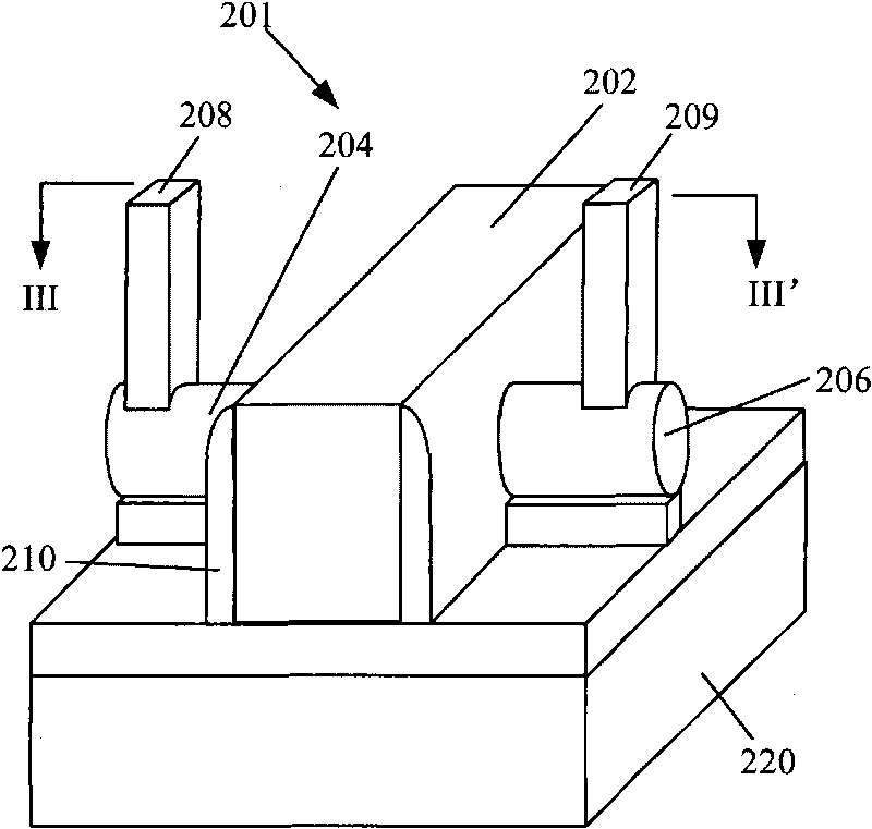
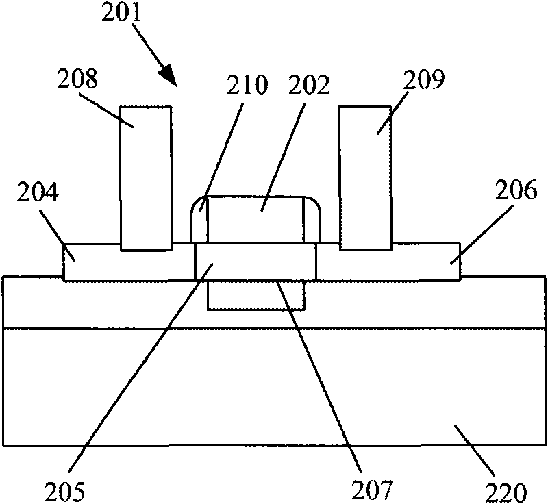
[0025] Such as figure 2 and image 3 As shown, the present embodiment provides a metal-semiconductor field effect transistor 201, which includes a metal gate 202 formed of metal and a cylindrical semiconductor material column 203 (refer to Figure 8 ). From one end to the other end of the semiconductor material pillar 203 is the source region 204 , the channel region 205 and the drain region 206 of the metal-semiconductor field effect transistor 201 . A through hole 207 is formed in the metal gate 202 , and the channel region 205 is located in the through hole 207 , that is, the metal gate 202 forms a wrap around the channel region 205 and exposes the source region 204 and the drain region 206 . The length of the channel region 205 is 5nm to 50nm. Correspondingly, the length of the metal gate 202 is less than or equal to the length of the...


PUM


Abstract

The invention relates to a metal-semiconductor field effect transistor, which comprises a grid electrode formed by metal, and a trench area which is made of a semiconductor material and is in Schottky contact with the grid electrode; the grid electrode is provided with a through hole inside; and at least part of the trench area is positioned in the through hole. Compared with the prior art, the meal grid electrode completely enclosing a trench area is formed in the metal-semiconductor field effect transistor so as to fully prevent the generation of leakage current.

Description

technical field [0001] The invention relates to the manufacturing field of semiconductor devices, in particular to a structure of a metal-semiconductor field-effect transistor. Background technique [0002] Metal-Semiconductor-Field-Effect-Transistor (MESFET) is a common transistor that is widely used in modern semiconductor devices. MESFET has current-voltage characteristics similar to Metal-Oxide-Semiconductor-Field-Effect-Transistor (MOSFE). However, in the gate part of the device, the MESFET uses a metal-semiconductor Schottky contact to replace the MOS structure of the MOSFET; and in the source and drain parts, the MESFET replaces the p-n junction in the MOSFET with an ohmic contact. MESFET, like other field effect devices, has a negative temperature coefficient at high current, that is, the current decreases with the increase of temperature. Therefore, even when using large-sized active devices or connecting many devices in parallel, thermal stability can still be ma...

Claims


Application Information

Patent Timeline
Patent Type & Authority Applications(China)
IPC IPC(8): H01L29/78H01L29/423
Inventor 肖德元季明华
Owner SEMICON MFG INT (SHANGHAI) CORP
Why Eureka
Try Eureka