Optical semiconductor apparatus and method for producing the same

A technology of an optical semiconductor device and a manufacturing method, which is applied to semiconductor devices, electric solid-state devices, electrical components, etc., can solve problems such as increased processing time, and achieve the effects of eliminating chip spatter and shortening reflow soldering time.

Active Publication Date: 2010-06-16
STANLEY ELECTRIC CO LTD
View PDF7 Cites 6 Cited by
  • Summary
  • Abstract
  • Description
  • Claims
  • Application Information

AI Technical Summary

Problems solved by technology

That is, it is necessary to set the temperature profile as follows: in the reflow process, before reaching the melting temperature of AuSn, keep it below the boiling point temperature of the solvent for a predetermined time, resulting in an increase in processing time

Method used


Image

  • Optical semiconductor apparatus and method for producing the same
  • Optical semiconductor apparatus and method for producing the same
  • Optical semiconductor apparatus and method for producing the same

Examples


Embodiment Construction

[0022] Next, embodiments of the optical semiconductor device of the present invention will be described with reference to the drawings. In addition, in the drawings shown below, substantially the same or equivalent constituent elements and parts are assigned the same reference numerals.

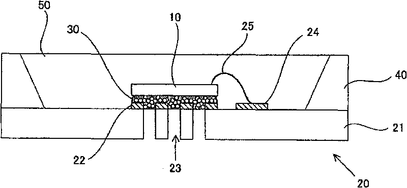
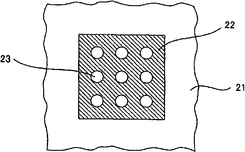
[0023] figure 2 It is a cross-sectional view showing the structure of an optical semiconductor device according to an embodiment of the present invention. image 3 It is a plan view of an underlayment forming part of a ceramic substrate constituting an optical semiconductor device.

[0024] The optical semiconductor device is composed of, for example, an LED chip 10 as an optical semiconductor element; a ceramic substrate 20 as a package substrate on which the LED chip 10 is mounted; a reflective member 40 disposed on the ceramic substrate 20 so as to surround the LED chip 10; and The light-transmitting resin portion 50 is provided to fill the space surrounded by the reflective member 40 a...


PUM


Abstract

An optical semiconductor apparatus can be configured by mounting an optical semiconductor element on a package substrate using a solder paste. The optical semiconductor apparatus can include a package substrate and a metal die pad formed on the substrate, and an optical semiconductor element bonded to the die pad with a solder material. The substrate can be made of a ceramic base material. A plurality of through holes can be formed in the substrate so that the through holes penetrate both the substrate base material and the die pad. Each of the through holes can have an inner surface where the ceramic base material is exposed. Each through hole can have an opening diameter greater than or equal to 40 [mu]m and less than or equal to 100 [mu]m. The plurality of through holes can be formed such that the total area of the openings of the through holes is 50% or less of the bonded area between the optical semiconductor element and the die pad including the through holes covered with the solder material. The through holes can be covered with the solder material at the upper end thereof where the optical semiconductor element and the die pad are bonded to each other.

Description

technical field [0001] The present invention relates to an optical semiconductor device and a manufacturing method thereof. Background technique [0002] figure 1 It is a cross-sectional view showing a configuration example of a conventional optical semiconductor device. The optical semiconductor device is composed of the following parts: a packaging substrate 200 such as a resin substrate; conductor wirings 201 and 202 that are provided on the surface of the packaging substrate 200 and are electrically insulated from each other; an optical semiconductor element 100 mounted on the conductor wiring 201; Above the optical semiconductor element 100 , a transparent cover 400 for protecting the optical semiconductor element 100 . The optical semiconductor 100 is electrically bonded to an underlay portion (not shown) located at an end portion of the conductor wiring 201 through a bonding material 300 . Furthermore, electrode pads (not shown) are provided on the upper surface of...

Claims


Application Information

Patent Timeline
Patent Type & Authority Applications(China)
IPC IPC(8): H01L33/48H01L33/62
CPCH01L2924/01322H01L33/486H01L2224/45144H01L33/62H01L2224/48091H01L2224/73265H01L2224/32225H01L2924/00014H01L2924/00
Inventor 近藤亮介酒井隆照
Owner STANLEY ELECTRIC CO LTD
Why Eureka
Try Eureka