

Topological structure of two-way DC/DC converter and converter
A topology and converter technology, applied in the direction of conversion equipment without intermediate conversion to AC, can solve the problems of reduced reliability, reduced reliability of equipment, and the inability to take into account the energy storage density of capacitors in both step-up and step-down gains.
- Summary
- Abstract
- Description
- Claims
- Application Information
AI Technical Summary
Problems solved by technology
Method used
Image

Examples
Embodiment 1
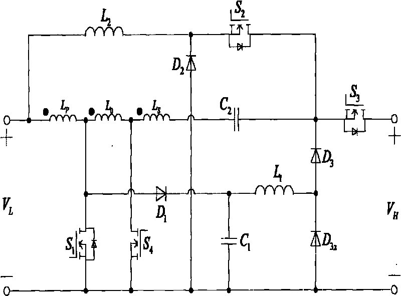
[0025] A bidirectional DC / DC converter topology, such as figure 1 As shown, including input terminal, output terminal, inductance L 1 and L 2 , coupled inductance L P , L O and L S , Diode D 1 、D 2 、D 3 and D 3X , FET S 1 , S 2 , S 3 and S 4 , capacitance C 1 and C 2 . The voltage at the input is V L , the voltage at the output is V H , inductance L 2 One end of the coupling inductor L P The terminal of the same name is connected to the positive pole of the input terminal, and the inductance L 2 The other end of the diode D 2 Negative electrode, field effect transistor S 2 source connection, the coupled inductor L P The opposite side of the coupled inductor L O The same name terminal, diode D 1 The positive electrode, field effect transistor S 1 connected to the drain, the coupled inductor L O Synonyms and L S The end of the same name, field effect transistor S 4 connected to the drain, the coupled inductor L S The opposite terminal of the capacitor...
Embodiment 2
[0092] A bidirectional DC / DC converter, the topology adopted is as follows figure 1 As shown, including input terminal, output terminal, inductance L 1 and L 2 , coupled inductance L P , L O and L S , Diode D 1 、D 2 、D 3 and D 3X , FET S 1 , S 2 , S 3 and S 4 , capacitance C 1 and C 2 . The voltage at the input is V L , the voltage at the output is V H , inductance L 2 One end of the coupling inductor L P The terminal of the same name is connected to the positive pole of the input terminal, and the inductance L 2 The other end of the diode D 2 Negative electrode, field effect transistor S 2 source connection, the coupled inductor L P The opposite side of the coupled inductor L O The same name terminal, diode D 1 The positive electrode, field effect transistor S 1 connected to the drain, the coupled inductor L O Synonyms and L S The end of the same name, field effect transistor S 4 connected to the drain, the coupled inductor L S The opposite termina...
PUM
| Property | Measurement | Unit |
|---|---|---|
| Capacitance | aaaaa | aaaaa |
| Capacitance | aaaaa | aaaaa |
Abstract
Description
Claims
Application Information