Direct laser pore-forming method

A laser and hole-forming technology, applied in welding equipment, laser welding equipment, metal processing equipment, etc., can solve the problems of ineffective implementation, low efficiency, complicated manufacturing process, etc., and achieve the effect of shortening the production process

Inactive Publication Date: 2010-06-23
PEKING UNIV FOUNDER GRP CO LTD +1
View PDF6 Cites 19 Cited by
  • Summary
  • Abstract
  • Description
  • Claims
  • Application Information

AI Technical Summary

Problems solved by technology

[0003] The traditional DLD technology uses browning as laser surface treatment, and then directly laser-forms holes on the copper foil. The process has weak processing capabilities: generally, it can only process copper foil with a thickness of a

Method used


Image

  • Direct laser pore-forming method
  • Direct laser pore-forming method
  • Direct laser pore-forming method

Examples


Embodiment Construction

[0021] The specific implementation method of the present invention will be further described below in conjunction with the embodiments.
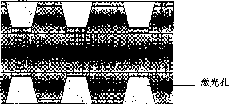
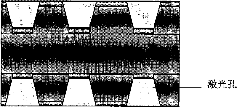
[0022] The idea of ​​the present invention is: before making the optical alignment point, the inner layer circuit is made first, and then pressed, and the optical alignment point is made by X-RAY drilling target. After the hole is formed, the smear should be removed first, and then the black film should be removed, and then transferred to the subsequent process.

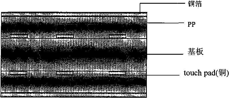
[0023] like figure 1 The above is a schematic diagram of the circuit board before forming holes. The specific method of forming holes is as follows:

[0024] The first step: optical alignment point design.

[0025] Due to the abnormal phenomenon of expansion and contraction in the production process of the sub-outer layer and the lamination, in order to improve the phenomenon of laser partial hole caused by expansion and contraction, the four corners of the board are designed and...


PUM

PropertyMeasurementUnit
Copper thicknessaaaaaaaaaa

Abstract

The invention discloses a direct laser pore-forming method. In order to control the thickness of copper foil in the range of requirements, a plurality of HDI manufacturing enterprises adopt a process technology of copper reduction but can not overcome the defect of the process technology for the processing thickness capability of the copper foil. The direct laser pore-forming method comprises the following steps: designing and manufacturing optical alignment points for processing circuit board blind holes; using the copper foil for layering press fit; adopting melanism for surface treatment; using target holes for positioning, carrying out laser-drilling, and processing optical alignment points for positioning; carrying out laser-drilling again, positioning by the processed optical alignment points, and positioning and processing the blind holes in a board. After press fit, the method carries out two procedures of film rubbing and melanism and enters the procedure of laser-drilling, so the production procedures are reduced by a half. Furthermore, the method can process the copper foil with the thickness of 9-12 Mum.

Description

technical field [0001] The invention relates to the field of high-density interconnect (HDI) production, in particular to a direct laser hole forming method. Background technique [0002] In the field of high-density interconnect (HDI) production, when using 1 / 3 oz or 1 / 2 oz copper foil for lamination for DLD (direct laser hole technology Copper foil direct laser drill: DLD), in order to make copper Foil thickness is controlled within the required range. Many HDI manufacturing companies have adopted copper-reducing process technology, but the defect in the ability of this process technology to process copper foil thickness has not been resolved. [0003] The traditional DLD technology uses browning as laser surface treatment, and then directly laser-forms holes on the copper foil. The process has weak processing capabilities: generally, it can only process copper foil with a thickness of about 7um. For copper foil with a thickness of more than 7um, the existing The technolo...

Claims


Application Information

Patent Timeline
IPC IPC(8): B23K26/38B23K26/18B23K26/42B23K26/382B23K26/70
Inventor 姚峰江辉王细心陈臣
Owner PEKING UNIV FOUNDER GRP CO LTD
Why Eureka
Try Eureka