

Lithography layout and method for measuring lithography deformation thereof
A layout and photolithography technology, applied in the field of semiconductor integrated circuit manufacturing equipment, can solve the problems of easy misjudgment, large dicing line layout area, and loss of function of rotation marks, and achieve the effect of improving deformation accuracy
- Summary
- Abstract
- Description
- Claims
- Application Information
AI Technical Summary
Problems solved by technology
Method used
Image

Examples
Embodiment Construction
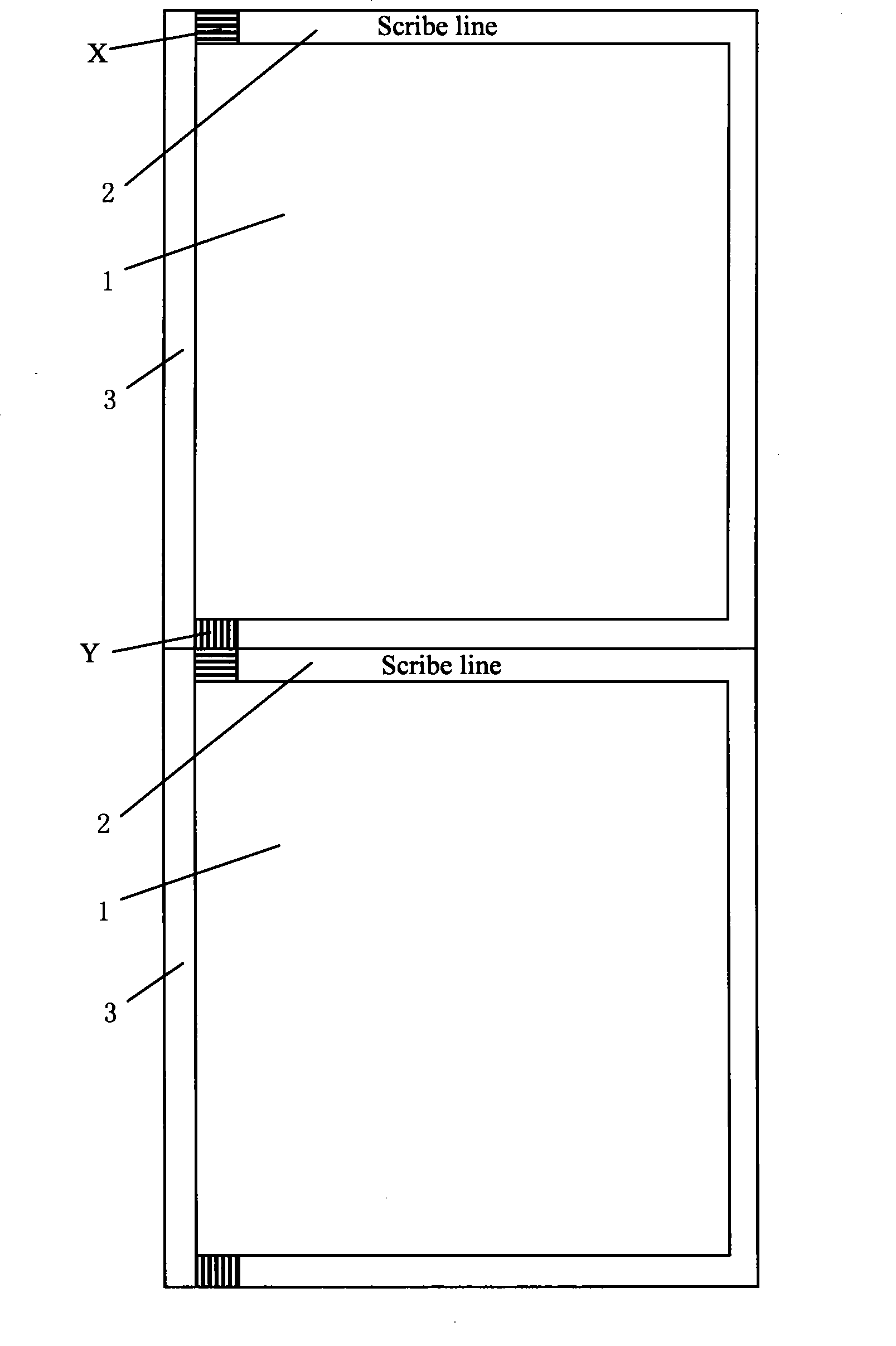
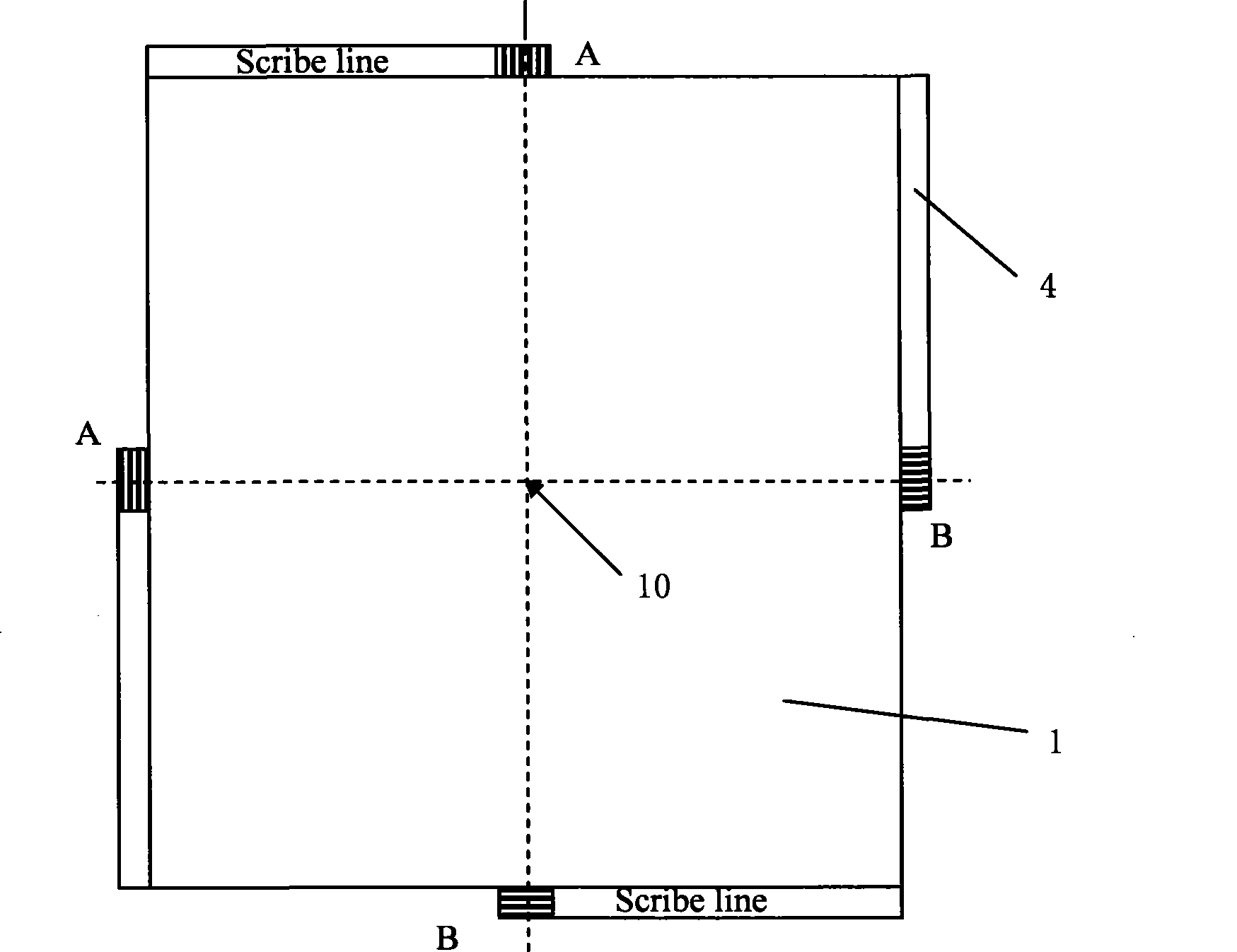
[0024] Such as image 3 As shown, the lithography layout of the present invention includes an exposure unit (shot) 1, and four scribe lines (Scribe Line) 4 around the exposure unit 1 are arranged in a windmill shape, that is, the four scribe lines 4 are respectively arranged on the four sides of the exposure unit 1 Above, each cutting line 4 starts from the vertex of the exposure unit 1 and ends at the midpoint of the side, and is arranged in sequence. The width of each cutting line 4 is in the range of 100 microns to 20 microns, which is half of the width of the cutting lines in the prior art.
[0025] The end of the cutting line 4 , that is, the cutting line 4 is overlaid with a rotation mark A or B at the midpoint of each side of the exposure unit 1 , and the rotation marks A and B are used as overlay marks. The rotation marks A, B are respectively aligned with the center 10 of the exposure unit (shot) 1 .
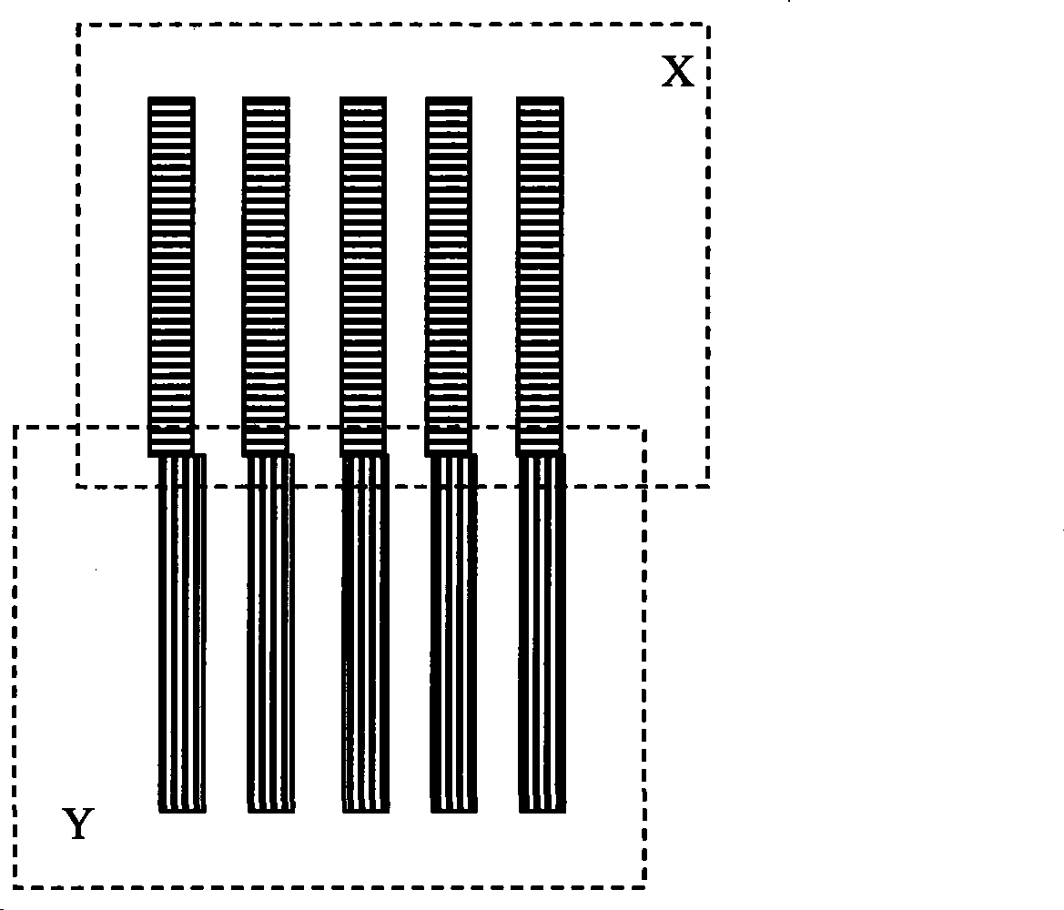
[0026] Such as Figure 6 As shown, the rotation mark A is a squ...
PUM
| Property | Measurement | Unit |
|---|---|---|
| width | aaaaa | aaaaa |
Abstract
Description
Claims
Application Information