Photosensitive conductive paste, and electrode and plasma display panel formed using the same
A conductive paste and photosensitivity technology, which is applied in the direction of conductive materials dispersed in non-conductive inorganic materials, gas discharge electrodes, conductors, etc., can solve the problem of increased electrode resistance and achieve the effect of cost reduction
Inactive Publication Date: 2010-06-23
TAIYO INK MFG
View PDF3 Cites 2 Cited by
- Summary
- Abstract
- Description
- Claims
- Application Information
AI Technical Summary
Problems solved by technology
However, if the electrode becomes thinner, there is a problem that the resistance value of the formed electrode increases
Method used
View moreImage
Smart ImageViewing Examples

Examples
Embodiment
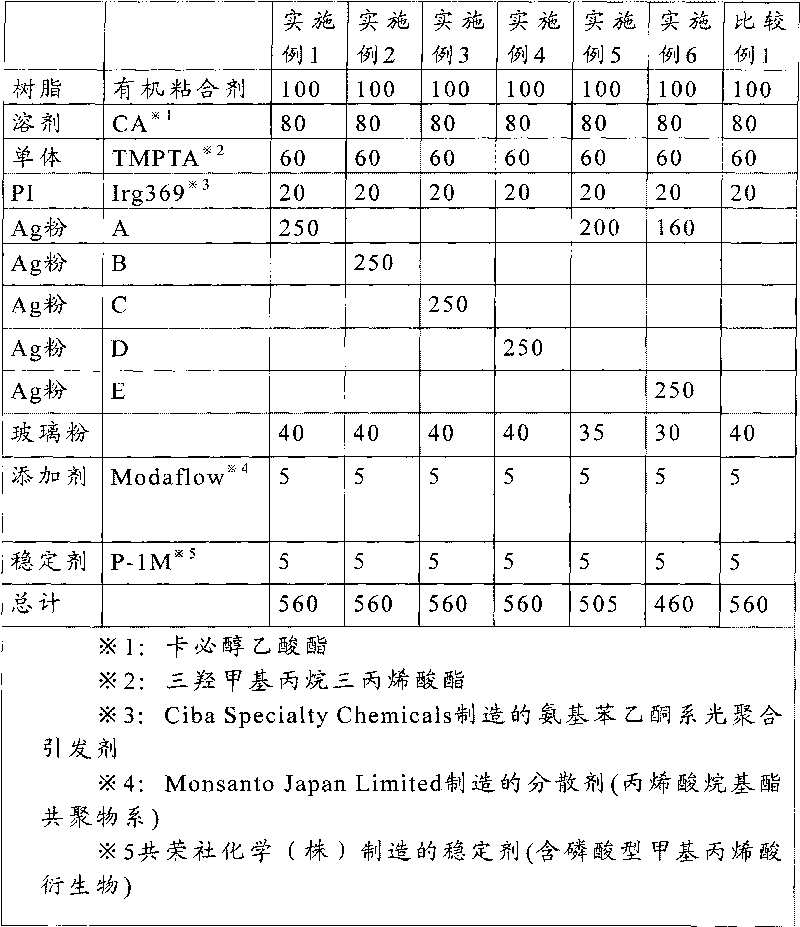
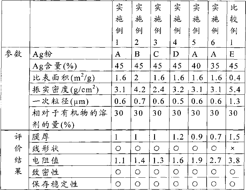
[0088] Examples and comparative examples are shown below to describe this embodiment concretely, but the present invention is not limited to the following examples.
[0089] Synthesis of Organic Binders
Login to View More PUM
| Property | Measurement | Unit |
|---|---|---|
| Particle size | aaaaa | aaaaa |
| Specific surface area | aaaaa | aaaaa |
| Tap density | aaaaa | aaaaa |
Abstract
The invention provides a photosensitive conductive paste capable of forming a film electrode with good linearity and compactness, and electrode and plasma display panel formed using the same. The photosensitive conductive paste is characterized in that the photosensitive conductive paste contains an organic binding agent, a silver powder, a photopolymerisable initiator, an organic solvent and glass powder, the primary particle size of the silver powder is below 1.0 mum, the specific surface area is 1.5 to 2.0 m<2> / g, and the tap density is 2.0 to 5.0 g / m<3>.
Description
technical field [0001] The present invention relates to, for example, a photosensitive conductive paste, an electrode, a plasma display panel, and a photosensitive conductive paste used for forming a high-definition electrode circuit on a substrate of a plasma display panel (hereinafter, abbreviated as "PDP"). Production method. Background technique [0002] As a method of forming patterns of conductors such as electrodes (hereinafter referred to as "electrodes") on printed circuit boards and PDP substrates (hereinafter referred to as "substrates"), the following screen printing method is generally used. In the screen printing method, a paste material in which metal powder is mixed with an organic binder is produced, and the paste material is printed on a substrate using a screen board to form electrodes. (For example, refer to Patent Document 1 and the like). [0003] In recent years, as the demands for miniaturization, thinning, high density, high definition, and high re...
Claims
Login to View More Application Information
Patent Timeline
 IPC IPC(8): H01J17/04H01J17/49H01J9/02G03F7/004H01B1/00H01B1/22H01B5/14H01B13/00H01J11/22H01J11/34
CPCH01B1/22H01J9/02H01J11/22H05K1/092
Inventor 伊藤秀之铃木信之
Owner TAIYO INK MFG
Features
- R&D
- Intellectual Property
- Life Sciences
- Materials
- Tech Scout
- Unparalleled Data Quality
- Higher Quality Content
- 60% Fewer Hallucinations
Learn More Browse by: Latest US Patents, China's latest patents, Technical Efficacy Thesaurus, Application Domain, Technology Topic, Popular Technical Reports.
© 2025 PatSnap. All rights reserved.Legal|Privacy policy|Modern Slavery Act Transparency Statement|Sitemap|About US| Contact US: help@patsnap.com