
Component cleaning method

A part and part of the technology, applied in the field of cleaning components, can solve the problems of pattern collapse, liquid can not be removed, etc., to achieve the effect of convenient cleaning

Inactive Publication Date: 2010-06-23
TOKYO ELECTRON LTD
View PDF2 Cites 6 Cited by
  • Summary
  • Abstract
  • Description
  • Claims
  • Application Information

AI Technical Summary

Problems solved by technology

[0004] However, in the rotary drying process, when the solution, purified water, etc. are volatilized, the interfacial tension of gas and liquid acts on the convex pattern formed on the wafer surface, causing pattern collapse.
In addition, when the wafer has a so-called Low-K film, liquid, pure water, etc. are easy to soak into the porous part of the Low-K film, and once immersed, the liquid cannot be completely removed.

Method used


Image

  • Component cleaning method
  • Component cleaning method
  • Component cleaning method

Examples


Embodiment Construction

[0054] Hereinafter, embodiments of the present invention will be described with reference to the drawings.

[0055] First, a method of cleaning components according to the first embodiment of the present invention will be described.

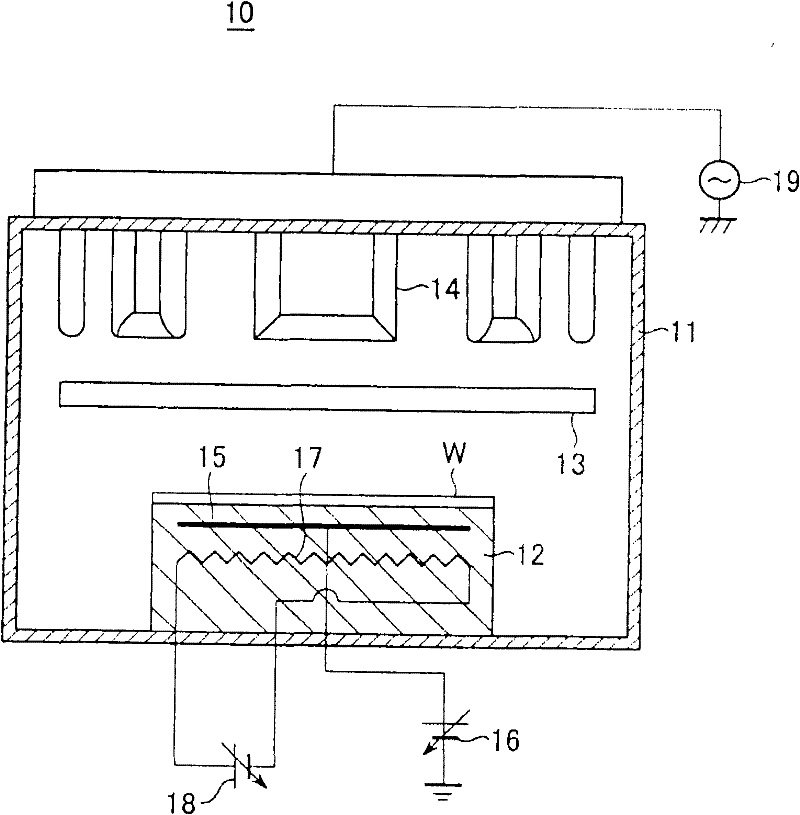
[0056] figure 1 It is a cross-sectional view schematically showing the structure of a wafer dry cleaning apparatus that executes the method for cleaning components according to this embodiment. This wafer dry cleaning apparatus removes foreign substances (hereinafter referred to as "particles") adhering to the surface of a semiconductor wafer (hereinafter simply referred to as "wafer") W without using a solvent or solution.

[0057] figure 1 Among them, the wafer dry-cleaning apparatus 10 (substrate processing apparatus) has: a processing chamber 11, a mounting table 12 provided at the inner bottom of the processing chamber 11, and a collecting plate 13 disposed above the mounting table 12 with a predetermined interval therebetween (configurati...


PUM


Abstract

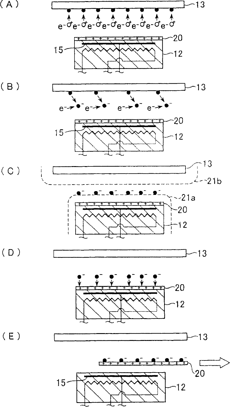
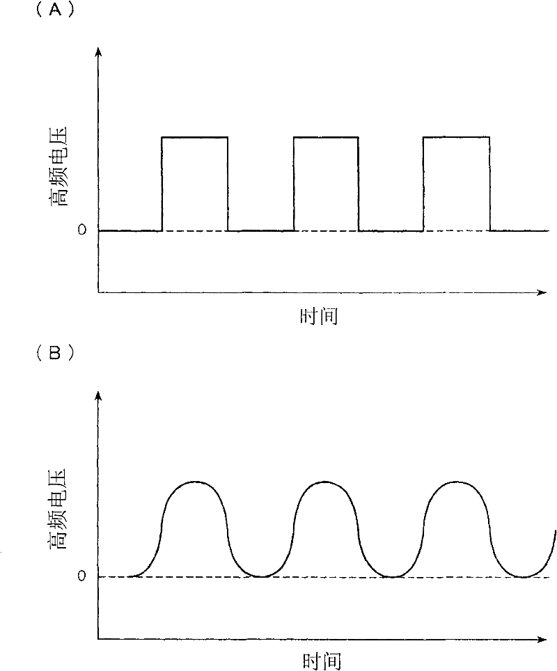
The invention provides a component cleaning method capable of preventing foreign substances from adhering to other components and cleaning the component conveniently. A wafer dry cleaning apparatus (10) comprises: a treatment chamber (11), a carrying bench (12) used for carrying wafer (W) disposed on the lower part in the treatment chamber (11), a adhered particles trapping plate (13) arranged relatively to the carrying bench (12) in the treatment chamber (11) and a plasma generation apparatus (14) used as a inductive coupling type plasma generation apparatus. The method comprises: moving a false wafer (20) into the treatment chamber (11); generating positive electric potential on the surface of the false wafer (20); generating surface wave plasma and stopping the generation of the surface wave plasma repeatedly on the false wafer (20) in the region nearer to the trapping plate; and moving the false wafer (20) out from the treatment chamber (11).

Description

technical field [0001] The present invention relates to a method for cleaning components, and more particularly, to a method for cleaning components using plasma to remove particles adhering to components of a substrate processing apparatus. Background technique [0002] As a method of cleaning semiconductor wafers after dry etching, for example, a wet substrate cleaning method is used: the wafer to be cleaned is soaked in a solution or a solvent or sprayed with a solvent or a solution to remove foreign matter such as particles, and then rinsed with pure water as necessary. rinse. [0003] In the wet substrate cleaning method, if a solvent or solution remains on the surface of the substrate after cleaning, it will cause watermarks, surface oxidation, etc. , Remove residual solution, purified water, etc. (For example, refer to Patent Document 1) [0004] However, in the spin drying process, when the solution, purified water, etc. are volatilized, the interfacial tension of...

Claims


Application Information

Patent Timeline
Patent Type & Authority Applications(China)
IPC IPC(8): H01L21/00B08B7/00
CPCY10S438/905Y10S438/906H01J37/32862H01L21/02057H01L21/302H01L21/3065H01L21/304
Inventor 守屋刚清水昭贵
Owner TOKYO ELECTRON LTD
Learn More