Ion injection method of a bag-shaped injection region and manufacture method of MOS (Metal Oxide Semiconductor) transistor

A MOS transistor and ion implantation technology, which is applied in the manufacture of MOS transistors and in the field of ion implantation, can solve problems such as junction leakage and achieve smooth threshold voltage Vt

Active Publication Date: 2010-06-23
SEMICON MFG INT (SHANGHAI) CORP
View PDF1 Cites 2 Cited by
  • Summary
  • Abstract
  • Description
  • Claims
  • Application Information

AI Technical Summary

Problems solved by technology

[0004] However, the doping ion species of the lightly doped drain (LDD) structure is different from the conductivity type of the semiconductor substrate or the doped well forming the MOSFET region, while the conductivity type of the pocket-shaped implanted region is different from that of the semiconductor substrate or The condu

Method used


Image

  • Ion injection method of a bag-shaped injection region and manufacture method of MOS (Metal Oxide Semiconductor) transistor
  • Ion injection method of a bag-shaped injection region and manufacture method of MOS (Metal Oxide Semiconductor) transistor
  • Ion injection method of a bag-shaped injection region and manufacture method of MOS (Metal Oxide Semiconductor) transistor

Examples


Embodiment Construction

[0029] The inventors of the present invention have found that when doping the pocket-shaped implanted region, the difference in the initial rotation angle will affect the junction capacitance and threshold voltage of the fabricated MOS transistor.

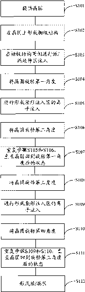
[0030] Based on the above considerations, in the following content of the specific embodiment, a method for manufacturing a MOS transistor is provided, such as figure 1 shown, including steps:

[0031] S101, providing wafers;

[0032] S102, forming a gate structure on the wafer;

[0033] S103, performing source / drain extension region implantation on both sides of the gate structure;

[0034] S104, rotating the wafer by a first angle;

[0035] S105, perform ion implantation to form a pocket-shaped implantation region;

[0036] S106, rotating the wafer by a second angle;

[0037] S107, repeat steps S105 and S106 until the wafer returns to the state after the first rotation angle;

[0038] S108, rotating the wafer at a third ang...


PUM


Abstract

The invention relates to an ion injection method of a bag-shaped injection region and a manufacture method of an MOS (Metal Oxide Semiconductor) transistor, wherein in the ion injection method for forming a bag-shaped injection region of an MOS transistor, the bag-shaped injection region is formed by twice multi-step rotations of ion injection, and the start angles of the twice multi-step rotations are different. Compared with the prior art, the invention can control the junction capacitance of the MOS transistor and ensure that the threshold voltage Vt of the manufactured MOS transistor is more smooth along with the change of Id, thereby being more beneficial to manufacturing MOS transistor in smaller sizes.

Description

technical field [0001] The invention relates to the manufacturing field of semiconductor devices, in particular to an ion implantation method for forming a pocket-shaped implantation region of a MOS transistor and a manufacturing method of the MOS transistor. Background technique [0002] Metal-oxide-semiconductor (MOS) transistors are the main driving force as semiconductor devices move toward high density and small size. The driving current and hot carrier injection are the two most important parameters in the design of MOS transistors. Traditional design achieves expected performance by controlling gate oxide, channel region, well region, source / drain extension doping shape, pocket implant region, source / drain implant shape and thermal budget, etc. . [0003] As the channel length of MOS devices becomes shorter, the source / drain depletion regions are too close to each other, which will lead to undesired punch through current and short channel effect. Therefore, those s...

Claims


Application Information

Patent Timeline
IPC IPC(8): H01L21/04H01L21/265H01L21/336
Inventor 赵猛王津洲
Owner SEMICON MFG INT (SHANGHAI) CORP
Why Eureka
Try Eureka