High-power photoconductivity switch test device and application thereof

A technology of photoconductive switch and test device, which is applied in the direction of measuring device, circuit breaker test, components of electrical measuring instrument, etc., can solve the problem of no patent or standard of switch test device, etc., and achieve compact structure and good high-voltage resistance performance. , to avoid the effect of breakdown

Active Publication Date: 2010-06-30
江苏先进无机材料研究院
View PDF3 Cites 9 Cited by
  • Summary
  • Abstract
  • Description
  • Claims
  • Application Information

AI Technical Summary

Problems solved by technology

However, to date there are no patents or standards related to such switch test devices

Method used


Image

  • High-power photoconductivity switch test device and application thereof
  • High-power photoconductivity switch test device and application thereof
  • High-power photoconductivity switch test device and application thereof

Examples


Embodiment Construction

[0058] The test device and test method of the present invention will be described in detail below in conjunction with the accompanying drawings. Those skilled in the art should understand that the present invention can also have many different forms without departing from the scope and essence of the present invention. The following specific embodiments are presented to make the disclosure more thorough and complete, so as to fully convey the scope of the present invention to those skilled in the art.

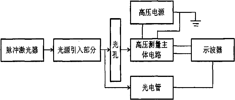
[0059] Such as figure 1 As shown, the high-power photoconductive switch testing device of the present invention includes: a pulsed laser, a light source introduction part, an optical hole, a high-voltage measurement main circuit, a high-voltage power supply, a photoelectric tube, and an oscilloscope; The laser pulse generated by the pulse laser is received by the light source introduction part to form a spot. The light source introduction part adjusts the optical path and regul...


PUM


Abstract

The invention relates to a high-power photoconductivity switch test device and application thereof. The test device comprises a pulse laser, a light source leading-in part, a light hole, a high-voltage measurement main circuit, a high-voltage power supply, an oscilloscope and a phototube, wherein the laser pulse generated by the pulse laser is received by the light source leading-in part to form light spots, and the light source leading-in part adjusts the light path and controls the light intensity of the light spots at unit area; the light spots are divided into measurement light spots and reference light spots by a spectroscope arranged in the light source leading-in part; the light hole receives the measurement light spots and adjusts the light intensity of the measurement light spots; the phototube receives and converts the reference light spots into electrical signals and transmits the electrical signals to the oscilloscope; the high-voltage measurement main circuit outputs electrical signals generated by the irradiation of the measurement light spots of a photoconductivity switch to be tested; the high-voltage power supply applies voltage to the high-voltage measurement main circuit; and the oscilloscope analyzes and displays the electrical signals from the high-voltage measurement main circuit.

Description

technical field [0001] The invention relates to a high-power photoconductive switch testing device and a method for testing parameters such as the response speed and dynamic resistance of the photoconductive switch by using the device, belonging to the technical field of high-voltage photoelectric device testing. Background technique [0002] Semiconductor photoconductive switches have attracted the attention of researchers of high-power switches due to their advantages of good stability, small size and easy integration. The first photoconductive switch prototype was prepared by D.H.Auston of Bell Labs in 1974. The material used was high-resistance Si, but the Si band gap was small and the critical breakdown field strength was low, so it could not be used to prepare high-voltage switches; In 1976, the first GaAs photoconductive switch was prepared by Chi H. Lee of the University of Maryland, and then the GaAs photoconductive switch became the focus of research in this field....

Claims


Application Information

Patent Timeline
Patent Type & Authority Applications(China)
IPC IPC(8): G01R31/327G01R1/02
Inventor 黄维常少辉陈之战施尔畏
Owner 江苏先进无机材料研究院
Why Eureka
Try Eureka