Inductor in semiconductor device packaging structure

A device packaging and packaging structure technology, applied in the field of inductance, can solve the problems of large influence of chip size, limited bonding wire inductance value, high cost, etc., achieve the effect of optimizing product performance, improving product integration, and reducing product cost

Inactive Publication Date: 2010-06-30
RDA TECH
View PDF0 Cites 6 Cited by
  • Summary
  • Abstract
  • Description
  • Claims
  • Application Information

AI Technical Summary

Problems solved by technology

[0003] In traditional integrated circuits, the application of inductors can generally be divided into the following three situations: the first application is to add off-chip inductors in the final manufacturing plant, this application method is not attractive, because the manufacturing plant has to The external inductance leaves assembly space, and the cost of the inductance must also be considered. At the same time, we need to use a certain length of off-chip wiring to connect the circuit chip to the off-chip inductance, which will generate additional parasitic
The second method is to use the bonding wire to form the inductance. The bonding wire is a very thin metal wire used to connect the circuit die and the package pin. The disadvantage of this method is that the inductance value provided by the bonding wire is limited. , and it has been shown that there is some electrical loss on the bonding wire
The third method is to draw the inductor on the circuit die. This method has a great impact on the size of the chip, the cost is high, and the Q value of the inductor is low.

Method used


Image

  • Inductor in semiconductor device packaging structure
  • Inductor in semiconductor device packaging structure
  • Inductor in semiconductor device packaging structure

Examples


Embodiment Construction

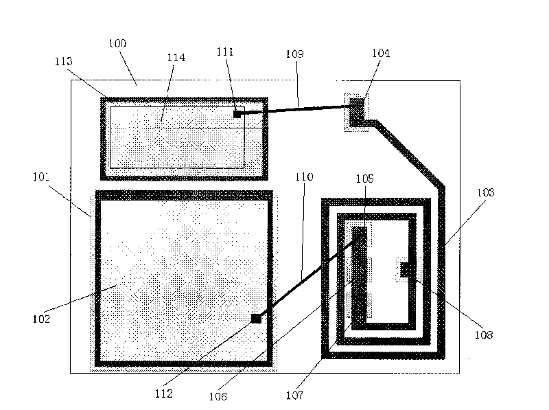
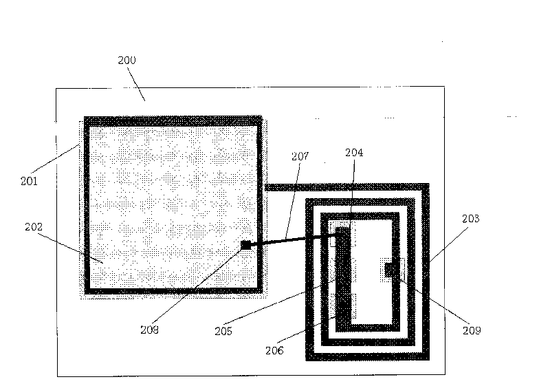
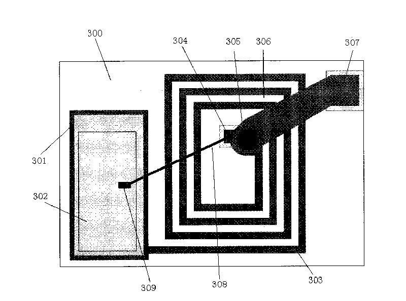
[0013] The invention discloses an inductor in a package structure of a semiconductor device. The semiconductor package structure includes a substrate and a plurality of circuit dies arranged on the substrate. A substrate bonding area is provided, the circuit die is provided with a circuit die bonding area, and the inductor is connected to circuit die bonds on two different circuit dies at least through the substrate bonding area and the bonding wire The bonding area is connected so that the inductor is connected to the circuit of the circuit die.

[0014] The inductor is planar spiral, or serpentine, or straight.

[0015] The planar spiral inductor is fully connected into the circuit die circuit.

[0016] The substrate is also provided with one or more substrate bonding areas in the middle of the inductor, and the part between any two substrate bonding areas on the inductor is connected to the circuit of the circuit die.

[0017] The substrate bonding area in the inductor is...


PUM


Abstract

The invention discloses an inductor in a semiconductor device packaging structure. The semiconductor packaging structure comprises a substrate and a circuit tube core arranged on the substrate, wherein the inductor is laid on the substrate, the planar spiral inductor is connected to a circuit of the circuit tube core, and the end part of the planar spiral inductor on the substrate is provided with a substrate bonding region. The inductor of the semiconductor device is integrated in the packaging structure through laying the planar spiral inductor on the substrate in the semiconductor packaging structure; and at the same time of improving the integration degree of products, the properties of the products are optimized, and the cost of the products is also reduced.

Description

technical field [0001] The invention relates to an inductor, in particular to an inductor arranged in a package structure of a semiconductor device. Background technique [0002] The field of wireless communication is facing the challenges of improving product integration, reducing product size and reducing product cost. The requirements for smaller, more complex and faster products not only challenge the design of circuit dies, but also The fabrication of various package structures presents new challenges. At present, the matching network, filter network and bias network in many radio frequency circuits require the inductor to have high inductance value and low loss value, that is, the inductor must have high Q characteristics. Generally, the higher the inductance value, the larger the size of the inductor, and the higher the cost. At the same time, the accuracy of the inductor is also proportional to the price of the inductor. In many circuit design applications, the indu...

Claims


Application Information

Patent Timeline
Patent Type & Authority Applications(China)
IPC IPC(8): H01L25/00H01L23/488H01L23/49H01L23/52H01L23/12
CPCH01L2224/48247H01L2224/48465H01L2924/30107
Inventor 陈俊谢利刚
Owner RDA TECH
Why Eureka
Try Eureka