
Semiconductor device

A semiconductor, conductive type technology, applied in the direction of semiconductor devices, electrical components, circuits, etc., can solve the problems of uniform potential distribution, different potentials, and the same total capacity of capacitors in the non-drift region 112.

Inactive Publication Date: 2010-07-07
ROHM CO LTD
View PDF5 Cites 10 Cited by
  • Summary
  • Abstract
  • Description
  • Claims
  • Application Information

AI Technical Summary

Problems solved by technology

Therefore, in the above-mentioned structure, although the capacity corresponding to the unit length in the circumferential direction of the floating plate can be made the same in each capacitor, the total capacity of the capacitor cannot be made the same.
As a result, the potentials between the opposing electrodes of each capacitor are actually different, and the potential distribution in the drift region 112 cannot be made uniform.

Method used


Image

  • Semiconductor device
  • Semiconductor device
  • Semiconductor device

Examples


Embodiment Construction

[0059] Hereinafter, embodiments of the present invention will be described in detail with reference to the drawings.

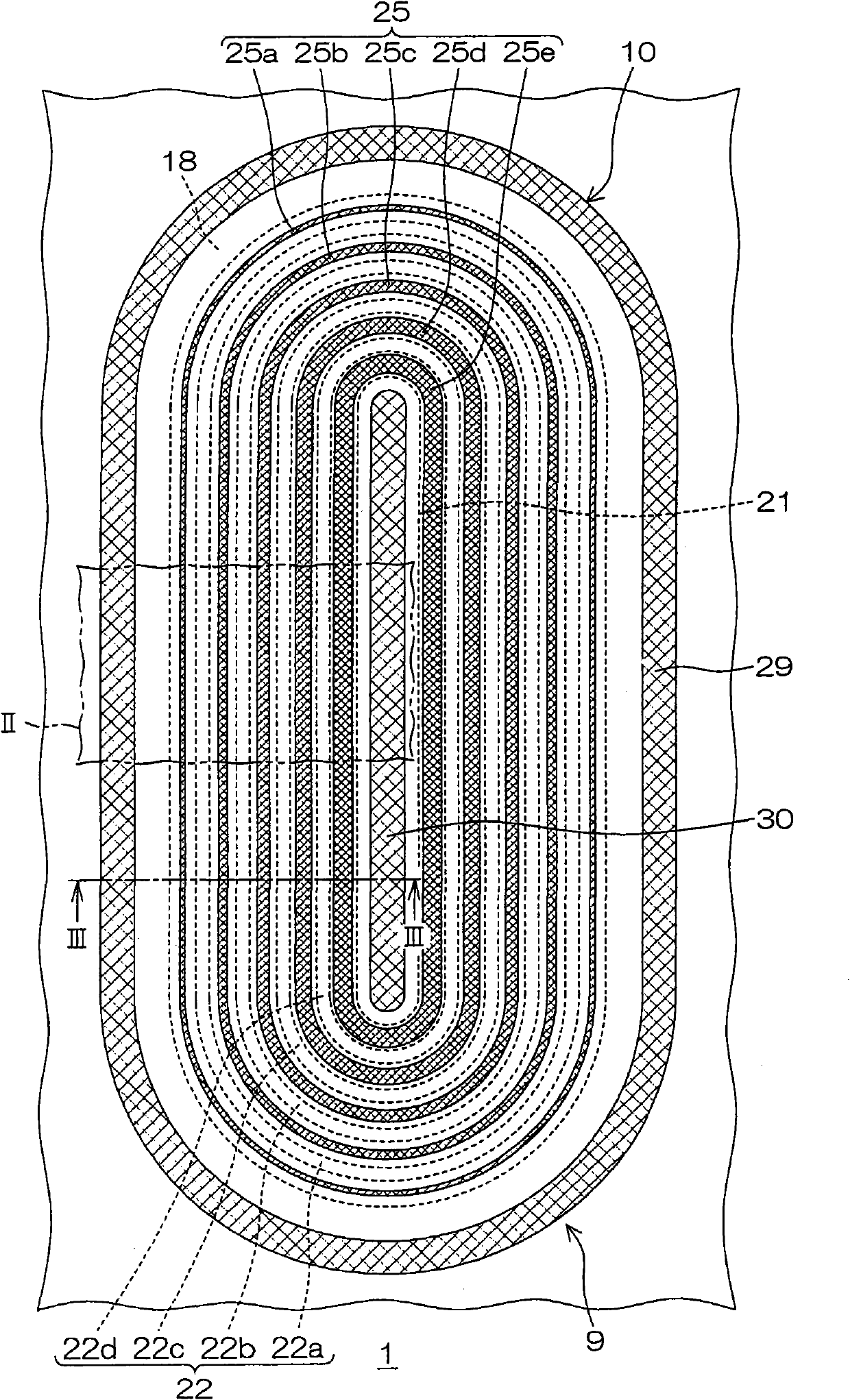
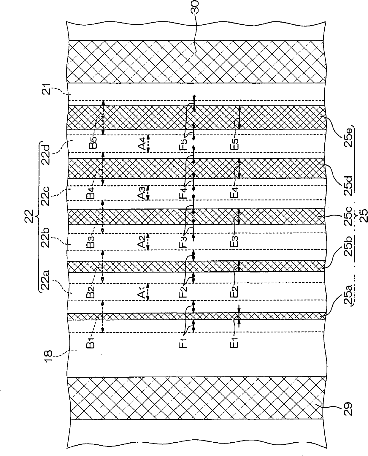
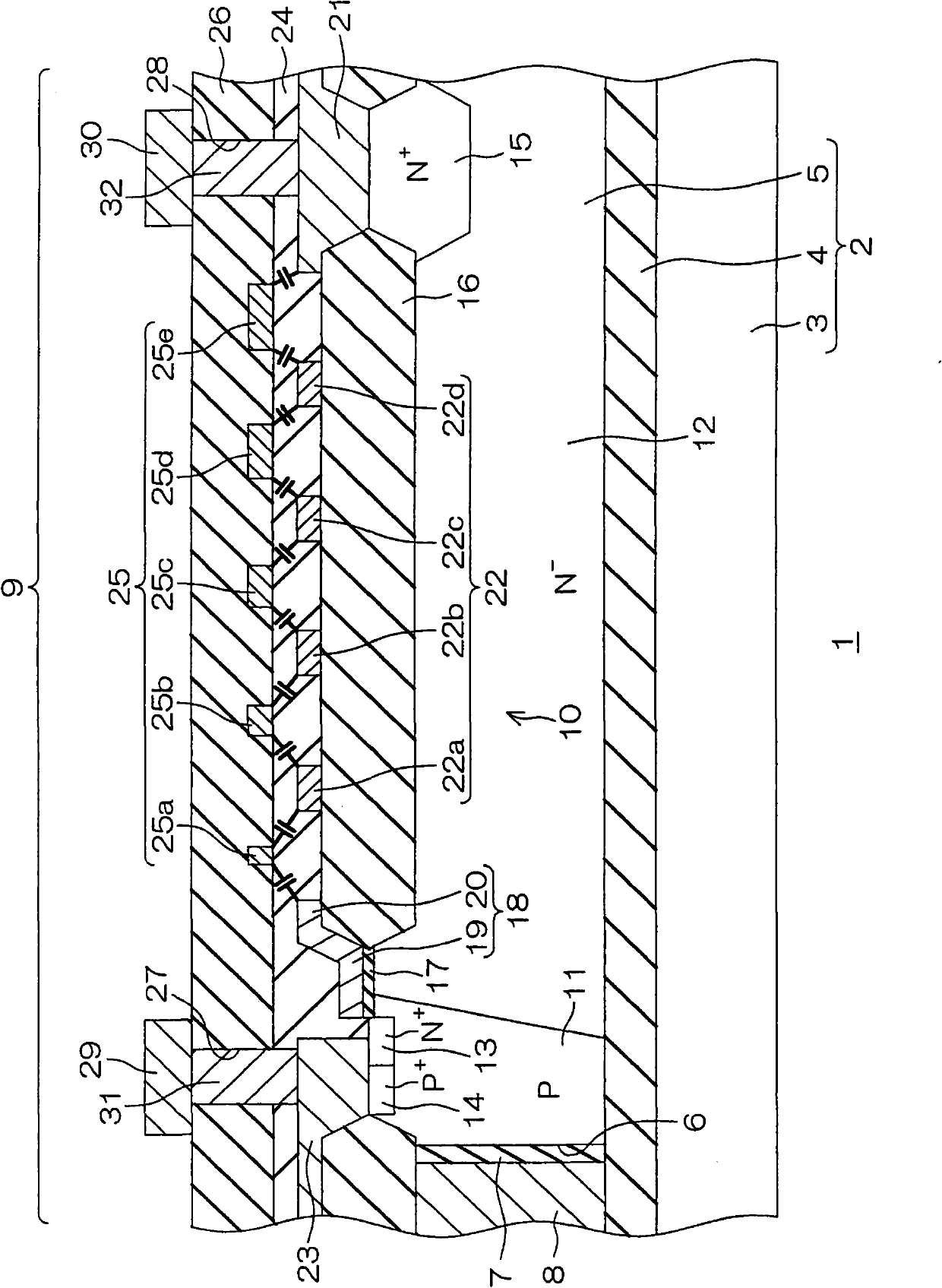
[0060] figure 1 It is a schematic plan view of the semiconductor device according to the first embodiment of the present invention. figure 2 for the reason figure 1 A magnified view of the area enclosed by Box II. image 3 for will figure 1 The cross-sectional view of the semiconductor device taken along the cutting line III-III.

[0061] The semiconductor device 1 includes a thick-film SOI substrate 2 . The thick-film SOI substrate 2 has a structure in which, on a silicon substrate 3, a BOX layer 4 made of silicon oxide is laminated as a BOX layer 4 made of silicon oxide. - Active layer 5 of the type semiconductor layer.

[0062] The layer thickness of the BOX layer 4 is, for example, 1 to 6 μm. The layer thickness of the active layer 5 is, for example, 10 to 50 μm. The N-type impurity concentration of the active layer 5 is, for example, 10 13 ~1...


PUM


Abstract

A semiconductor device comprises: a semiconductor layer; a first conductivity type first impurity region; a second conductivity type body region; a first conductivity type second impurity region; a field insulating film; a gate insulating film; a first floating plate provided in the form of a ring having a constant width on the field insulating film; and a second floating plate provided in the form of a ring having a constant width on the same layer above the first floating plate, wherein the first floating plate and the second floating plate are formed by not less than three in total so that the peripheral lengths at the centers in the width direction thereof are entirely different from one another, alternately arranged in plan view so that the one having a relatively smaller peripheral length is stored in an inner region of the one having a relatively larger peripheral length, and formed to satisfy the relational expression: L / d=constant (L: the outer periphery of the inner one of the first and second floating plates adjacent to each other in plan view, d: the distance between the outer periphery of the plate defining L and the inner periphery of the first or second floating plate adjacent to the plate to be opposed to the outer periphery thereof).

Description

technical field [0001] The present invention relates to a semiconductor device. Background technique [0002] Conventionally, LDMOSFETs are known as high withstand voltage elements used in power MOSFETs. [0003] Figure 10 It is a schematic cross-sectional view of a semiconductor device including a conventional LDMOSFET. [0004] The semiconductor device 101 includes a thick-film SOI substrate 102 . The thick-film SOI substrate 102 has a structure in which a N - type active layer 105 is laminated. [0005] In the active layer 105 , a deep groove 106 is formed penetratingly in the layer thickness direction, and the depth is from the surface of the active layer 105 to the BOX layer 104 . The inner surface of the deep groove 106 is covered with a silicon oxide film 107 . [0006] The inside of silicon oxide film 107 is filled with polysilicon 108 . As a result, an element formation region 109 is formed on the active layer 105, surrounded by the deep groove 106, and insul...

Claims


Application Information

Patent Timeline
Patent Type & Authority Applications(China)
IPC IPC(8): H01L29/78H01L29/06
CPCH01L29/402H01L29/42368H01L29/7824H01L29/404H01L29/0696
Inventor 中川义和
Owner ROHM CO LTD
Learn More