A Superjunction Taped Groove Transversal Voltage Sustainability Region with Resistive Field Plate
A technology of lateral withstand voltage and field plate, which is applied in the direction of semiconductor devices, electrical components, circuits, etc., can solve the problems of destroying the electric field distribution on the surface of the withstand voltage region, the advantages of super junction technology cannot be fully exerted, and the destruction of charge balance conditions, etc., to achieve Effect of high resistivity, good uniformity, optimized relationship
- Summary
- Abstract
- Description
- Claims
- Application Information
AI Technical Summary
Problems solved by technology
Method used
Image
Examples
Embodiment 1
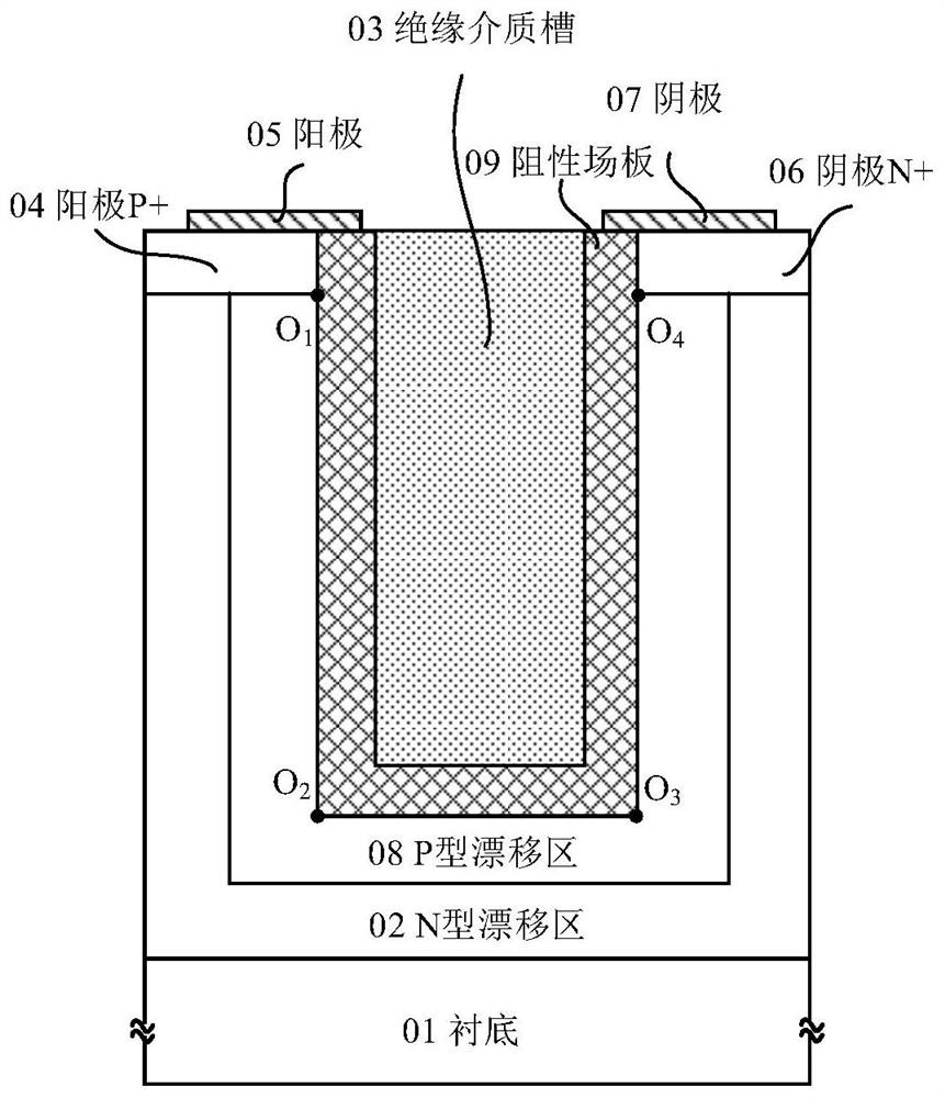
[0028] This embodiment provides a superjunction grooved lateral voltage withstand region with a resistive field plate, the structure of which is as follows image 3 As shown; including: substrate 01, N-type drift region 02, insulating medium tank 03, P+ anode region 04, anode 05, N+ cathode region 06, cathode 07, P-type drift region 08 and resistive field plate 09; wherein, The N-type drift region 02 is disposed on the substrate 01, the P-type drift region 08 is disposed in the N-type drift region 02, the insulating dielectric groove 03 is disposed in the P-type drift region 08, and the P+ anode region 04 and N+ cathode region 06 are respectively arranged on both sides of the insulating medium tank 03, and are located above the N-type drift region 02 and the P-type drift region 08, the anode 05 is arranged on the P+ anode region 04, and the cathode 07 is arranged On the N+ cathode region 06 ; the resistive field plate 09 is set between the insulating medium groove 03 and the P...
Embodiment 2
[0041] This embodiment provides another superjunction grooved lateral voltage withstand region with a resistive field plate, the structure of which is as follows Figure 12 Shown; Its difference with embodiment 1 is: also be provided with a layer of insulating dielectric buffer layer 10 between described resistive field plate 09 and P-type drift region; Described insulating dielectric buffer layer 10 can adopt and insulating dielectric groove ( 03) is filled with the same dielectric material as the dielectric material, or another dielectric material, the purpose of which is to play the role of buffer protection for the implementation of the resistive field plate.
PUM
| Property | Measurement | Unit |
|---|---|---|
| thickness | aaaaa | aaaaa |
| electrical resistivity | aaaaa | aaaaa |
| electrical resistivity | aaaaa | aaaaa |
Abstract
Description
Claims
Application Information


