
LiNbO3/SiO2/diamond multilayer piezoelectric film and preparation method thereof

A diamond and piezoelectric film technology, applied in the manufacture/assembly of piezoelectric/electrostrictive devices, piezoelectric/electrostrictive/magnetostrictive devices, circuits, etc., can solve the temperature stability of multi-layer film structure SAW devices Sexuality has not been improved, etc.

Inactive Publication Date: 2011-09-14
ZHENGZHOU UNIV
View PDF1 Cites 0 Cited by
  • Summary
  • Abstract
  • Description
  • Claims
  • Application Information

AI Technical Summary

Problems solved by technology

Due to LiNbO 3 , ZnO, Al 2 o 3 The frequency temperature coefficient TCF of diamond and diamond is less than zero (the temperature delay coefficient TCD is greater than zero), so ZnO, Al 2 o 3 The temperature stability of SAW devices with multi-layer film structure as buffer layer has not been improved

Method used


Image

  • LiNbO3/SiO2/diamond multilayer piezoelectric film and preparation method thereof
  • LiNbO3/SiO2/diamond multilayer piezoelectric film and preparation method thereof

Examples


Embodiment 1

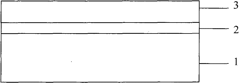
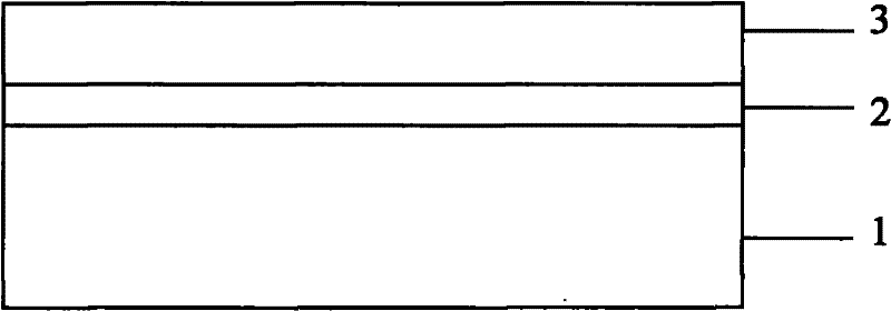
[0010] 1. Put the diamond substrate (which can be cleaned before use) into the vacuum chamber of the pulsed laser deposition equipment, and evacuate to 10 -3 Pa, heat the substrate to 300°C, use silicon (Si) as the target, the distance between the target and the diamond substrate is 4.5cm, feed 99.99% high-purity oxygen, and the oxygen pressure is 15Pa. Amorphous SiO deposited on the bottom 2 Buffer layer, amorphous SiO 2 The thickness of the buffer layer is 0.13μm;

[0011] 2. Amorphous SiO will be deposited 2 The diamond substrate of the buffer layer was heated up to 680°C, 99.99% high-purity oxygen was introduced during the deposition process, the oxygen pressure was kept at 60Pa, and the laser frequency was 3Hz. LiNbO 3 As the target, the distance between the target and the diamond substrate is 4cm, and the single pulse energy density is 3.5J / cm 2 laser on amorphous SiO 2 Deposit LiNbO with a thickness of 0.45 μm on the buffer layer 3 Piezoelectric film layer;

[00...

Embodiment 2

[0014] 1. Put the diamond substrate (which can be cleaned before use) into the vacuum chamber of the pulsed laser deposition equipment, and evacuate to 10 -3 Pa, heat the diamond substrate to 350°C, use silicon as the target, and conduct SiO in a 99.99% high-purity oxygen atmosphere at 15Pa 2 Deposition, the distance between the target and the substrate is 5.7cm, and the pulsed laser is used to deposit amorphous SiO with a thickness of 0.3μm on the diamond substrate. 2 The buffer layer;

[0015] 2. Amorphous SiO will be deposited 2 The diamond substrate of the buffer layer was heated up to 640°C, 99.99% high-purity oxygen was introduced during the deposition process, the oxygen pressure was kept at 40Pa, and the laser frequency was 3Hz. LiNbO 3 As a target, the distance between the target and the diamond substrate is 4.5cm, and the single pulse energy density is 4J / cm 2 laser on amorphous SiO 2 Deposit LiNbO with a thickness of 0.6 μm on the buffer layer 3 Piezoelectric f...


PUM

PropertyMeasurementUnit
thicknessaaaaaaaaaa
surface roughnessaaaaaaaaaa

Abstract

The invention relates to a LiNbO3 / SiO2 / diamond multilayer piezoelectric film and a preparation method thereof, efficiently solving the problems of the temperature stability of surface acoustic wave (SAW) devices and preparation of high c-axis orientated LiNbO3 thin film. The technical scheme of the invention is as follows: an amorphous SiO2 buffering layer is introduced between a diamond substrate and a LiNbO3 piezoelectric thin film. The preparation method comprises the following steps of: firstly, taking silicon as a target material on the diamond substrate, and depositing the amorphous SiO2 on the diamond substrate by a pulse laser deposition method to form an amorphous SiO2 buffering layer; secondly, heating the prepared amorphous SiO2 / diamond substrate, taking the LiNbO3 as the target material, and depositing the LiNbO3 on the amorphous SiO2 buffering layer by the pulse lasers to form a composite piezoelectric thin film having the amorphous SiO2 buffering layer between the LiNbO3piezoelectric thin film layer and the diamond substrate; and cooling down the layer to 18-25 DEG C after the LiNbO3 piezoelectric thin film layer is deposited. The invention has simple structure, advanced and scientific method and high temperature stability, and improves the working frequency of the SAW devices.

Description

1. Technical field [0001] The present invention relates to piezoelectric thin film materials, especially a kind of LiNbO 3 / SiO 2 / Diamond multilayer piezoelectric film and preparation method thereof. 2. Background technology [0002] With the rapid development of mobile communication technology, the frequency of use of surface acoustic wave (SAW) devices has been continuously increased, from the initial MHz level to the current GHz level. It is well known that the improvement of the operating frequency of SAW devices is mainly achieved by shortening the interdigital electrode period or using high-sonic materials, but for traditional surface acoustic wave materials such as LiNbO 3 , LiTaO 3 Due to the low surface wave velocity of materials such as single crystal materials or PZT series piezoelectric ceramics, it is quite difficult to reach the operating frequency of GHz under the current process conditions. Therefore, the development of high-sonic materials has become a t...

Claims


Application Information

Patent Timeline
Patent Type & Authority Patents(China)
IPC IPC(8): H01L41/083H01L41/22H10N30/50H10N30/05
Inventor 王新昌田四方王俊喜贾建峰
Owner ZHENGZHOU UNIV
Learn More